FEDR44V064B-02
MR44V064B
10/16
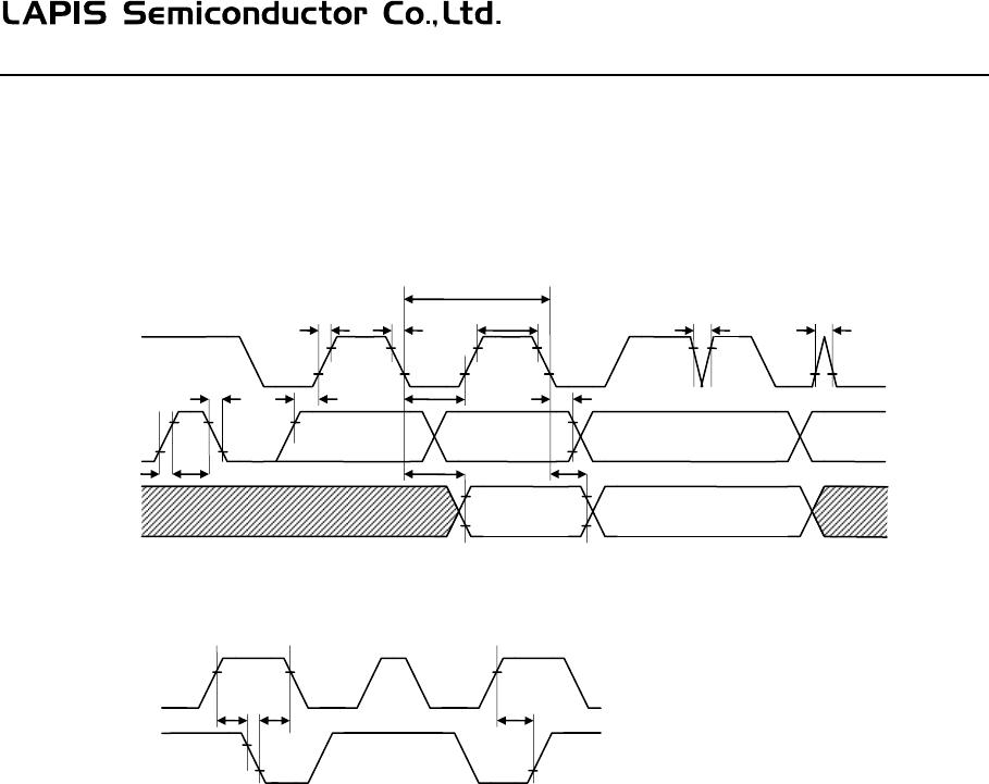
AC CHARACTERISTICS
V
CC
=Max. to Min., Ta=Topr.
Parameter Symbol
F/S-mode
F/S-mode
Plus
HS-mode Unit Note
Min. Max. Min. Max. Min. Max.
Clock frequency
f
SCL
D.C. 400 D.C. 1000 DC 3400 KHz
Clock Low time tLOW 1300 500 160 ns
Clock High time tHIGH 600 300 60 ns
Output Data delay time tAA 900 450 130 ns
BUS release time before transfer start tBUF 1300 500 300 ns
Start condition hold time tHD:STA 600 250 160 ns
Start condition setup time tSU:STA 600 250 160 ns
Input data hold time tHD:DAT 0 0 0 ns
Input data setup time tSU:DAT 100 100 10 ns
SDA, SCL rise time tR 300 300 80 ns 1
SDA, SCL fall time tF 300 100 80 ns 1
Stop condition setup time tSU:STO 600 250 160 ns
Output data hold time tDH 0 0 0 ns
Noise removal time (SDA, SCL) tSP 50 50 5 ns
Note: 1. Not 100% tested
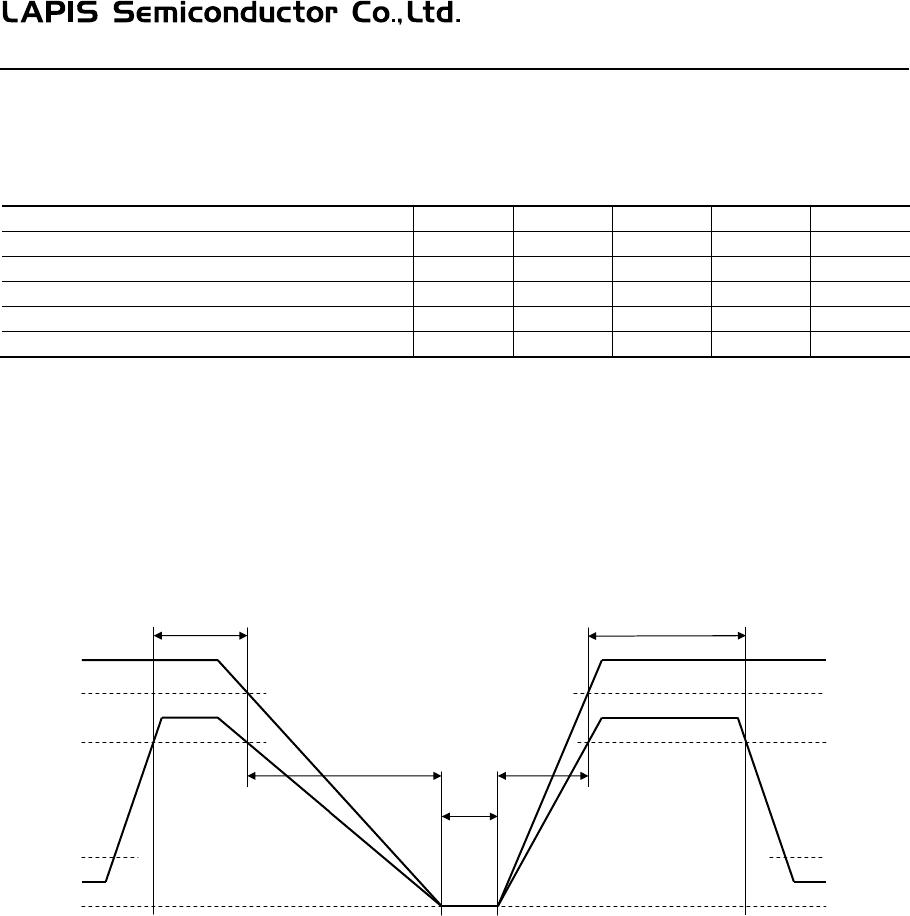
Equivalent AC Load Circuit
3.3V
1.1kΩ
Out
ut
100pF