FEDR44V064B-02
MR44V064B
4/16
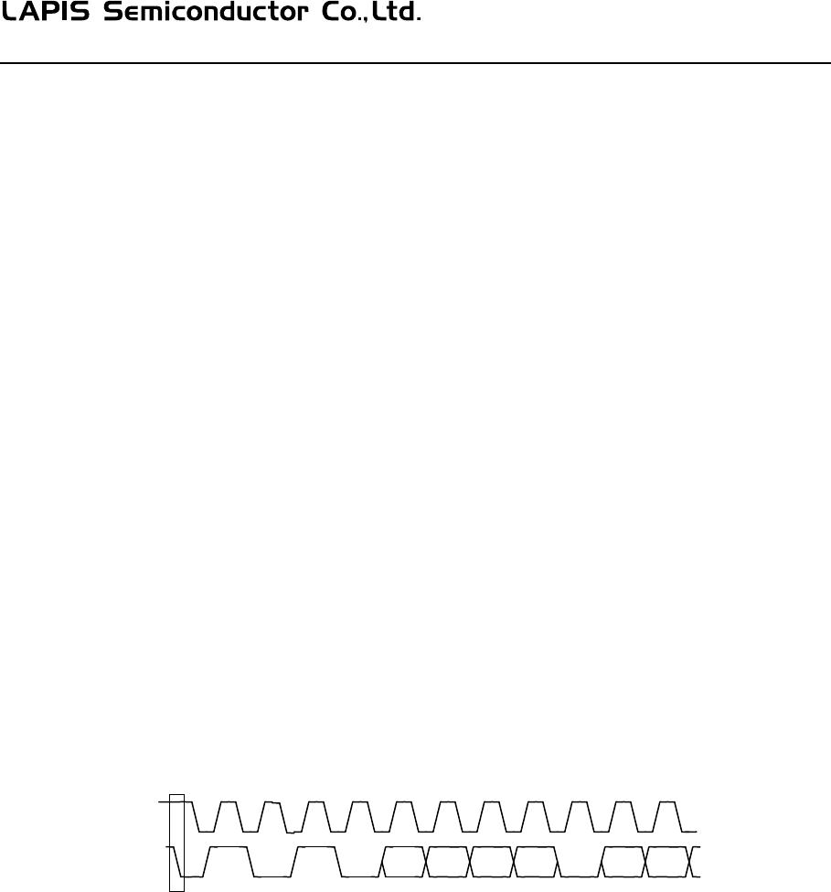
ACKNOWLEDGE ( ACK ) SIGNAL
This acknowledge ( ACK ) signal is a software rule to show whether data transfer has been made normally or not.
In master and slave, the device (μ-COM at slave address input of write command, read command, and this IC at
data output of read command) at the transmitter (sending) side releases the bus after output of 8bit data.
The device (this IC at slave address input of write command, read command, and μ-COM at data output of read
command) at the receiver (receiving) side sets SDA “LOW” during 9 clock cycles, and outputs acknowledge
signal ( ACK signal) showing that it has received the 8bit data.
This IC, after recognizing start condition and slave address (8bit), outputs acknowledge signal ( ACK signal)
“LOW”.
Each write action outputs acknowledge signal ( ACK signal ) “LOW”, at receiving 8bit data ( word address and
write data ).
Each read action outputs 8bit data ( read data ), and detects acknowledge signal ( ACK signal ) “LOW”.
When acknowledge signal ( ACK signal ) is detect, and stop condition is not sent from the master (μ-COM) side,
this IC continues data output. When acknowledge signal ( ACK signal ) is not detected, this IC stops data
transfer, and recognizes stop condition ( stop bit ), and ends read action. And this IC gets in status.
SLAVE ADDRESS
Output slave address after start condition from master.
The significant 4 bits of slave address are used for recognizing a device type. The device code of this IC is fixed
to “1010”.
Next slave addresses (A2 A1 A0 … device address) are for selecting devices, and plural ones can be used on a
same bus according to the number of device addresses.
The most insignificant bit (R/W…READ/WRITE) of slave address is used for designating write or read action,
and is as shown below.
Setting R/W to 0 write (setting 0 to word address setting of random read)
Setting R/W to 1 read
WRITE PROTECT
When WP terminal is set Vcc(H level), data rewrite of all addresses is prohibited. When it is set Vss(L level),
data rewrite of all address is enabled. Be sure to connect this terminal to Vcc or Vss, or control it to H level or L
level. Because this terminal is pulled down internally, in the case of Open the terminal will be recognized as L
level
During write cycle WP terminal must be always “L” level. WP terminal must be fixed from start condition to
stop condition.
SCL
SDA
START
condition
2 3
ACK
56 89741 12
1 0 01
A
2
A
1
A
0R/W
FEDR44V064B-02
MR44V064B
5/16
COMMAND
BYTE WRITE CYCLE
Arbitrary data is written to FeRAM. When to write only 1 byte, byte write is normally used.
start condition
slave address with LSB is 0 (write)
1
st
and 2
nd
word address
byte of write data.
stop condition
PAGE WRITE CYCLE
When to write continuous data of 2 bytes or more, simultaneous write is possible by page write cycle. The
address reaches the final address, the address will be rolled over to the first address. By page write cycle, up to
8,192 bytes data can be written. When data above the maximum bytes are sent, data from the first byte will be
overwritten.
BYTE WRITE CYCLE ( HS-MODE )
The MR44V064B support a maximum 3.4MHz high speed mode. When HS-mode operation is needed, the
HS-mode command is required before any command. After the HS-mode command is issued, MR44V064B will
be the HS-mode, until stop condition is issued.
1 0 A2 A1 A0 1 0
Slave address
S
T
A
R
T
W
R
I
T
E
1
s
t
WORD address 2
n
d
WORD address
W
A
8
W
A
7
W
A
0
W
A
12
D
7
D
0
S
T
O
P
A
C
K
A
C
K
A
C
K
A
C
K
Write data
0 0 1 X X 0 0
HS-mode command
S
T
A
R
T
N
A
C
K
X 0 0 0
1 0 A2 A1 A0 1 0
Slave address
S
T
A
R
T
W
R
I
T
E
1
s
t
WORD address 2
n
d
WORD address
W
A
8
W
A
7
W
A
0
W
A
12
D
7
D
0
S
T
O
P
A
C
K
A
C
K
A
C
K
A
C
K
Write data
0 0 0
1 0 A2 A1 A0 1 0
Slave address
S
T
A
R
T
W
R
I
T
E
1
s
t
WORD address 2
n
d
WORD address
W
A
8
W
A
7
W
A
0
W
A
12
D
7
D
0
S
T
O
P
A
C
K
A
C
K
A
C
K
A
C
K
D
7
D
0
A
C
K
Write data Write data
0 0 0
FEDR44V064B-02
MR44V064B
6/16
RANDOM READ CYCLE
Random read cycle is a command to read data by designating address.
start condition
slave address with LSB is 0 (write)
1
st
and 2
nd
word address
start condition
slave address with LSB is 1 (read)
read out byte of data.
ACK to “H
stop condition
SEQUENTIAL READ CYCLE
When ACK signal “L” after D0 is detected, and stop condition is not sent from master side, the next address data
can be read in succession. The address reaches the final address, the address will be rolled over to the first
address.
CURRENT READ CYCLE
Current read cycle is a command to read data of internal address register without designating address. When the
last read or write address is (n)-th address just before current read cycle, the current read command outputs data
of (n+1)-th address. The previous read or write sequence should be complete up to stop condition.
Just after POWER ON, the internal address resister is unstable.
CURRENT ADDRESS READ CYCLE ( HS-MODE )
The MR44V064B support a maximum 3.4MHz high speed mode. When HS-mode operation is needed, the
HS-mode command is required before any command. After the HS-mode command is issued, MR44V064B will
be the HS-mode, until stop condition is issued.
1 0 A2 A1 A0 1 0
Slave address
S
T
A
R
T
W
R
I
T
E
1
s
t
WORD address 2
n
d
WORD address
W
A
8
W
A
7
W
A
0
W
A
12
D
7
D
0
S
T
O
P
A
C
K
A
C
K
A
C
K
Read data
1 0 A2 A1A010
Slave address
S
T
A
R
T
R
E
A
D
A
C
K
D
7
A
C
K
D
0
N
A
C
K
0 0 0
1 0 A2 A1 A0 1 0
Slave address
S
T
A
R
T
W
R
I
T
E
1
s
t
WORD address 2
n
d
WORD address
W
A
8
W
A
7
W
A
0
W
A
12
D
7
D
0
S
T
O
P
A
C
K
A
C
K
A
C
K
Read data
1 0 A2 A1A010
Slave address
S
T
A
R
T
R
E
A
D
A
C
K
N
A
C
K
0 0 0
0 0 1 X X 0 0
HS-mode command
S
T
A
R
T
Read data
D0
D7
S
T
O
P
N
A
C
K
N
A
C
K
1 0 A2 A1 A0 1 0
Slave address
S
T
A
R
T
R
E
A
D
A
C
K
X
1 0 A2 A1 A0 1 0
Slave address
S
T
A
R
T
R
E
A
D
Read data
D0
D7
S
T
O
P
N
A
C
K
A
C
K

MR44V064BMAZAATL

Mfr. #:
Manufacturer:
Description:
F-RAM FeRAM/64Kbit 8Kb x 8 8pin SOP 3.4MHz
Lifecycle:
New from this manufacturer.
Delivery:
DHL FedEx Ups TNT EMS
Payment:
T/T Paypal Visa MoneyGram Western Union

Products related to this Datasheet