CYIFS782BSXC

Low EMI Spectrum Spread Clock
FS781/82/84
Cypress Semiconductor Corporation 198 Champion Court San Jose, CA 95134-1709 408-943-2600
Document #: 38-07029 Rev. *F Revised January 2, 2005
Features
Spread Spectrum clock generator (SSCG) with 1×, 2×,
and 4× outputs
6- to 82-MHz operating frequency range
Modulates external clocks including crystals, crystal
oscillators, or ceramic resonators
Programmable modulation with simple R-C external
loop filter (LF)
Center spread modulation
3V-5V power supply
TTL-/CMOS-compatible outputs
Low short-term jitter
Low-power Dissipation
3.3 VDC = 37 mW – typical
5.0 VDC = 115 mW – typical
Available in 8-pin SOIC and TSSOP packages
Applications
Desktop/notebook computers
Printers, copiers, and MFP
Scanners and fax
LCD displays and monitors
CD-ROM, VCD, and DVD
Automotive and embedded systems
Networking, LAN/WAN
Digital cameras and camcorders
•Modems
Benefits
Programmable EMI reduction
Fast time to market
Lower cost of compliance
No degradation in rise/fall times
Lower component and PCB layer count
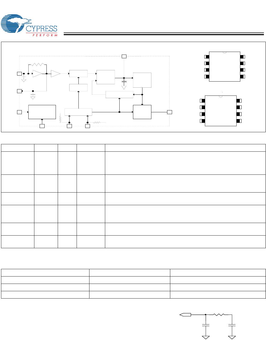
Functional Description
The Cypress FS781/82/84 are Spread Spectrum clock
generator ICs (SSCG) designed for the purpose of reducing
electromagnetic interference (EMI) found in today’s
high-speed digital systems.
The FS781/82/84 SSCG clocks use a Cypress-proprietary
technology to modulate the input clock frequency, XIN, by
modulating the frequency of the digital clock. By modulating
the reference clock the measured EMI at the fundamental and
harmonic frequencies of FSOUT is greatly reduced. This
reduction in radiated energy can significantly reduce the cost
of complying with regulatory requirements without degrading
digital waveforms.
The Cypress FS781/82/84 clocks are very simple and
versatile devices to use. By programming the two range select
lines, S0 and S1, any frequency from 6- to 82-MHz operating
range can be selected. The FS781/2/4 are designed to
operate over a very wide range of input frequencies and
provides 1×, 2×, and 4× modulated clock outputs.
The FS78x devices have a simple frequency selection table
that allows operation from 6 MHz to 82 MHz in four separate
ranges. The bandwidth of the frequency spread at FSOUT is
determined by the values of the loop filter components. The
modulation rate is determined internally by the input frequency
and the selected input frequency range.
The Bandwidth of these products can be programmed from as
little as 1.0% up to as much as 4.0% by selecting the proper
loop filter value. Refer to the Loop Filter Selection chart in
Table 2 and Table 3 for the recommended values. Due to a
wide range of application requirements, an external loop filter
(LF) is used on the FS78x products. The user can select the
exact amount of frequency modulation suitable for the appli-
cation. Using a fixed internal loop filter would severely limit
the use of a wide range of modulation bandwidths (Spread %)
to a few discrete values. Refer to FS791/2/4 products for appli-
cations requiring 80- to 140-MHz frequency range.
[+] Feedback
FS781/82/84
Document #: 38-07029 Rev. *F Page 2 of 12
Output Frequency Selection
Loop Filter Selection Chart
The following table provides a list of recommended loop filter
values for the FS781/82/84. The FS78X is divided into four
ranges and operated at both 3.3V and 5.5 VDC. The loop filter
at the right is representative of the loop filter components in
Table 2.
Pin Description
Pin Name I/O Type Description
1/2 (SOIC)
3/4 (TSSOP)
X
IN
/X
OUT
I/O Analog Pins form an on-chip reference oscillator when connected to terminals
of an external parallel resonant crystal. X
IN
may be connected to
TTL/CMOS external clock source. If X
IN
is connected to an external clock
other than crystal, leave X
OUT
(pin 2) unconnected.
7/3 (SOIC)
1/5 (TSSOP)
S0 / S1 I CMOS/TTL Digital control inputs to select input frequency range and output
frequency scaling. Refer to Table 2 and Table 3 for selection. S0 has internal
pull-down. S1 has internal pull-up.
4 (SOIC)
6 (TSSOP)
LF I Analog Loop Filter. Single ended three-state output of the phase detector. A two-pole
passive loop filter is connected to LF.
6 (SOIC)
8 (TSSOP)
FSOUT O CMOS/TTL Modulated Clock Frequency Output. The center frequency is the same as
the input reference frequency for FS781. Input frequency is multiplied by 2×
and 4× for FS782 and FS784, respectively.
8 (SOIC)
2 (TSSOP)
V
DD
P Power Positive Power Supply.
5 (SOIC)
7 (TSSOP)
V
SS
P Power Power Supply Ground.
Table 1. FSOUT SSCG (Modulated Output Clock) Product Selection
Product Number FSOUT Frequency Scaling Description
FS781 1× modulated frequency of input clock
FS782 2× modulated frequency of input clock
FS784 4× modulated frequency of input clock
Block Diagram
Pin Configuration
Phase
Detector
VCO
1(3)
2(4)
Xin
Xout
10 pF.
Reference
Divider
8 pF
8 pF
250 K
VCO / N
Modulation
Control
Input Control Logic
Output
Divider
and
Mux
Power Contol
Logic
3(5)
7(1)
8(2)
5(7)
4(6)
VDD
S0S1
FSOUT
Loop Filter
VSS
6(8)
VSS
VDD
(TSSOP Pin #)
1
2
3
4
8
7
6
5
Xin
Xout
S1
LF
VDD
S0
FSOUT
VSS
FS78x
8 Pin SOIC Package
1
2
3
4
8
7
6
5
S0
VDD
Xin
Xout
FSOUT
VSS
LF
S1
FS78x
8 Pin TSSOP Package
C8
R6
C7
LF (pin 4)
[+] Feedback
FS781/82/84
Document #: 38-07029 Rev. *F Page 3 of 12
Table 2. FS781/82/84 Recommended Loop Filter Values C7 (pF) @ +3.3 VDC ±5% (R6 = 3.3K)
[1, 2, 3, 4]
Input MHz S1 S0 BW = 1.0%
[3]
BW = 1.5%
[3]
BW = 2.0%
[3]
BW = 2.5%
[3]
BW = 3.0%
[3]
BW = 3.5%
[3]
BW = 4.0%
[3]
6 0 0 10,000/1000 1550 910 780 700 640 560
8 0 0 10,000/330 990 820 640 520 450 400
10 0 0 1040 680 460 360 300 240 210
12 0 0 830 420 300 220 200 190 170
14 0 0 580 230 200 160 140 100 80
16 0 1 10000 980 760 580 470 410 385
18 0 1 1200 750 580 470 415 370 300
20 0 1 1000 730 470 390 320 220 190
22 0 1 960 640 410 270 230 200 180
24 0 1 920 400 250 210 180 160 150
26 0 1 660 300 220 180 150 140 120
28 0 1 470 230 180 150 130 100 70
30 0 1 470 180 140 120 100 80 60
32 0 1 330 170 120 100 82 68 47
34 1 0 10000 860 640 520 430 380 330
36 1 0 2200 820 620 470 400 330 290
38 1 0 1500 690 520 410 340 290 240
40 1 0 960 600 420 340 280 220 160
42 1 0 940 620 380 275 230 210 180
44 1 0 950 680 400 250 210 190 170
46 1 0 900 580 270 220 190 180 165
48 1 0 790 440 260 210 180 160 140
50 1 0 660 360 250 190 170 150 140
52 1 0 470 325 220 185 155 135 120
54 1 0 470 270 200 170 140 130 100
56 1 0 445 250 185 150 120 85 47
58 1 0 430 210 165 130 100 65 33
60 1 0 295 185 150 120 100 90 82
62 1 0 270 220 150 120 100 82 68
64 1 1 1180 860 560 410 340 290 230
65 1 1 1180 850 540 400 330 280 220
66 1 1 1180 760 560 350 260 220 210
68 1 1 1180 750 500 320 260 230 210
70 1 1 1120 740 470 370 300 240 170
72 1 1 1160 780 470 300 250 220 190
74 1 1 1110 770 470 280 230 210 190
76 1 1 1000 720 440 240 210 190 170
78 1 1 910 670 270 210 190 170 160
80 1 1 900 620 260 210 190 170 156
82 1 1 900 540 250 210 190 170 150
Notes:
1. If the value selected from the above chart is not a standard, use the next available larger value.
2. All bandwidths indicated above are total peak-to-peak spread. 1% = +0.5% to –0.5%. 4% = +2.0% to –2.0%.
3. If C8 is not listed in the chart for a particular bandwidth and frequency, it is not used in the loop filter.
4. Contact Cypress for LF values less than 1.0% bandwidth.
[+] Feedback

CYIFS782BSXC

Mfr. #:
Manufacturer:
Cypress Semiconductor
Description:
Phase Locked Loops - PLL Reduction SSCGs COM
Lifecycle:
New from this manufacturer.
Delivery:
DHL FedEx Ups TNT EMS
Payment:
T/T Paypal Visa MoneyGram Western Union