CYIFS782BSXC

FS781/82/84
Document #: 38-07029 Rev. *F Page 4 of 12
Table 3. FS781/82/84 Recommended Loop Filter Values C7 (pF) @ +5.0 VDC ±5% (R6 = 3.3K)
[1, 2, 3, 4]
Input MHz S1 S0 BW = 1.0%
[3]
BW = 1.5%
[3]
BW = 2.0%
[3]
BW = 2.5%
[3]
BW = 3.0%
[3]
BW = 3.5%
[3]
BW = 4.0%
[3]
6 0 0 1140 1030 930 830 710 610 510
8 0 0 1170 970 740 570 460 400 280
10 0 0 1030 660 430 350 280 210 130
12 0 0 760 340 230 200 180 160 130
14 0 0 450 240 180 140 100 70 50
16 0 1 2490 970 730 590 480 430 370
18 0 1 2490 870 650 510 430 370 310
20 0 1 1360 680 480 370 280 190 250
22 0 1 990 560 330 260 230 200 190
24 0 1 820 360 250 200 180 160 150
26 0 1 530 270 210 170 150 110 90
28 0 1 430 230 180 150 110 100 90
30 0 1 250 200 150 110 100 90 80
32 1 0 Note 4 1000 740 570 470 410 370
34 1 0 Note 4 990 710 520 420 360 300
36 1 0 Note 4 970 670 480 380 310 230
38 1 0 Note 4 880 560 380 310 270 220
40 1 0 Note 4 800 460 290 240 230 220
42 1 0 1030 680 360 260 220 200 190
44 1 0 790 560 260 220 200 190 170
46 1 0 1110 420 280 210 180 170 140
48 1 0 1110 280 200 190 170 140 120
50 1 0 830 330 200 180 160 130 110
52 1 0 560 340 205 170 140 120 90
54 1 0 510 280 180 140 110 110 90
56 1 0 470 210 160 120 100 90 90
58 1 0 450 220 250 110 90 80 80
60 1 0 430 240 120 90 80 80 70
62 1 1 Note 4 800 580 430 330 250 180
64 1 1 Note 4 720 490 375 285 200 140
66 1 1 Note 4 630 400 320 240 150 100
68 1 1 Note 4 690 365 285 225 170 140
70 1 1 Note 4 650 330 250 210 190 180
72 1 1 Note 4 575 340 250 210 190 170
74 1 1 Note 4 500 355 245 205 180 165
76 1 1 Note 4 550 330 230 200 175 160
78 1 1 Note 4 600 290 220 190 170 155
80 1 1 Note 4 570 240 210 185 165 150
82 1 1 Note 4 540 250 200 180 160 140
[+] Feedback
FS781/82/84
Document #: 38-07029 Rev. *F Page 5 of 12
SSCG Modulation Profile
The digital control inputs S0 and S1 determine the modulation
frequency of FS781/2/4 products. The input frequency is
divided by a fixed number, depending on the operating range
that is selected. The modulation frequency of the FS78x can
be determined from Table 4. To compute the modulation
frequency, determine the values of S0 and S1, and find the
modulation divider number in Table 4.
Theory of Operation
The FS781/82/84 devices are phase-locked loop-(PLL)-type
clock generators using Direct Digital Synthesis (DDS). ‘By
precisely controlling the bandwidth of the output clock, the
FS781/2/4 products become a low-EMI clock generator. The
theory and detailed operation of these products will be
discussed in the following sections.
EMI
All clocks generate unwanted energy in their harmonics.
Conventional digital clocks are square waves with a duty cycle
that is very close to 50%. Because of the 50/50 duty cycle,
digital clocks generate most of their harmonic energy in the
odd harmonics (e.g., third, fifth, seventh). It is possible to
reduce the amount of energy contained in the fundamental
and harmonics by increasing the bandwidth of the funda-
mental clock frequency. Conventional digital clocks have a
very high Q factor, which means that all of the energy at that
frequency is concentrated in a very narrow bandwidth, conse-
quently, higher energy peaks. Regulatory agencies test
electronic equipment by the amount of peak energy radiated
from the equipment. By reducing the peak energy at the funda-
mental and harmonic frequencies, the equipment under test is
able to satisfy agency requirements for EMI. Conventional
methods of reducing EMI have been to use shielding, filtering,
multi-layer PCBs, etc. These FS781/2 and 4 reduce the peak
energy in the clock by increasing the clock bandwidth and
lowering the Q of the clock.
SSCG
The FS781/82/84 products use a unique method of modulating
the clock over a very narrow bandwidth and controlled rate of
change, both peak to peak and cycle to cycle. The FS78x
products take a narrow band digital reference clock in the
range of 6–82 MHz and produce a clock that sweeps between
a controlled start and stop frequency and precise rate of
change. To understand what happens to an SSCG clock,
consider that we have a 20-MHz clock with a 50% duty cycle.
From a 20-MHz clock we know the following:
Clock Frequency = Fc = 20 MHz.
Clock Period = Tc = 1/20 MHz = 50 ns.
Consider that this 20-MHz clock is applied to the X
IN
input of
the FS78x as either an externally driven clock or the result of
a parallel resonant crystal connected to pins 1 and 2 of the
FS78x. Also consider that the products are operating from a
5V DC power supply and the loop filter is set for a total
bandwidth spread of 2%. Refer to Figure 2.
Table 4. Modulation Rate Divider Ratios
S1 S0 Input Frequency Range (MHz) Modulation Divider Number
0 0 6 to 16 120
0 1 16 to 32 240
1 0 32 to 66 480
1 1 66 to 82 720
Xin
+ .5%
- .5%
TIME (microseconds)
1.0%
Total
Figure 1. Frequency Profile in Time Domain
[5]
Note:
5. With the correct loop filter connected to Pin 4, the following profile will provide the best EMI reduction. This profile can be seen on a Time Domain Analyzer.
[+] Feedback
FS781/82/84
Document #: 38-07029 Rev. *F Page 6 of 12
From the above parameters, the output clock at FSOUT will be
sweeping symmetrically around a center frequency of 20 MHz.
The minimum and maximum extremes of this clock will be
+200 kHz and –200 kHz. So we have a clock that is sweeping
from 19.8 MHz to 20.2 MHz and back again. If we were to look
at this clock on a spectrum analyzer we would see the picture
in Figure 3. Keep in mind that this is a drawing of a perfect
clock with no noise.
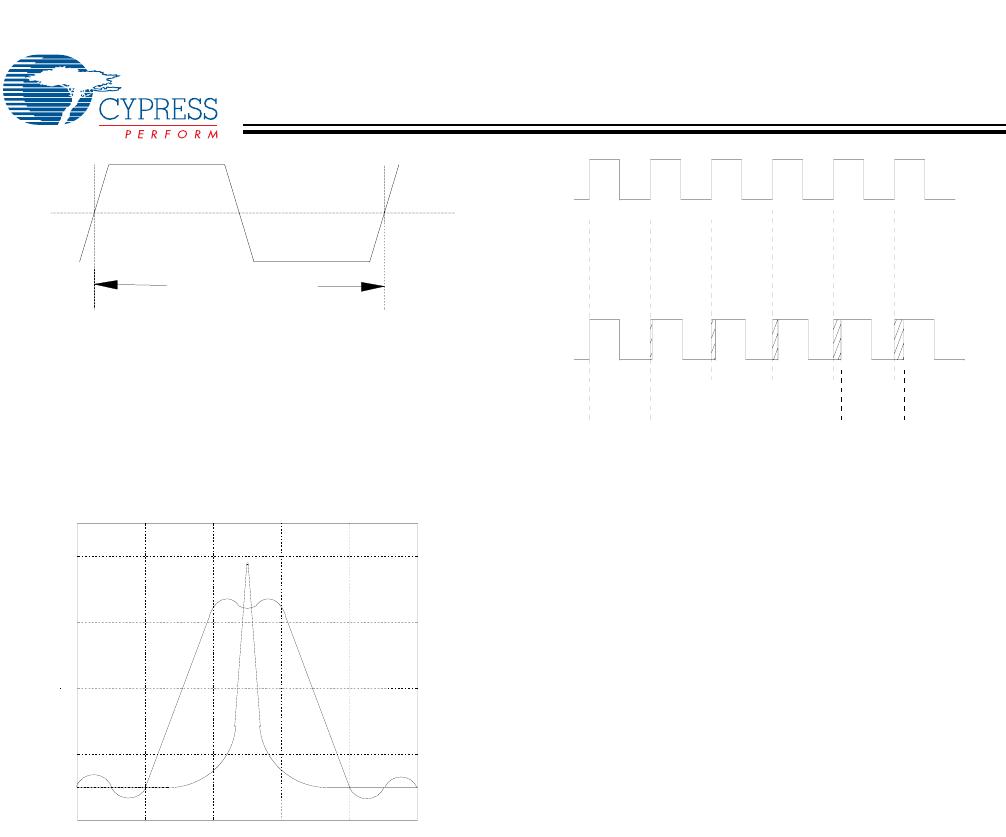
We see that the original 20-MHz reference clock is at the
center frequency (Cf), and the min. and max. extremes are
positioned symmetrically about the center frequency. This type
of modulation is called Center-Spread. Figure 4 shows a
20-MHz clock as it would be seen on an oscilloscope. The top
trace is the non-modulated reference clock. The bottom trace
is the modulated clock at pin 6. From this comparison chart
you can see that the frequency is decreasing and the period
of each successive clock is increasing. The Tc measurements
on the left and right of the bottom trace indicate the max. and
min. extremes of the clock. Intermediate clock changes are
small and accumulate to achieve the total period deviation.
The reverse of this figure would show the clock going from
minimum extreme back to the high extreme.
Looking at Figure 3, you will note that the peak amplitude of
the 20-MHz non-modulated clock is higher than the wideband
modulated clock. This difference in peak amplitudes between
modulated and unmodulated clocks is the reason why SSCG
clocks are so effective in digital systems. This figure refers to
the fundamental frequency of a clock. A very important charac-
teristic of the SSCG clock is that the bandwidth of the funda-
mental frequency is multiplied by the harmonic number. In
other words, if the bandwidth of a 20-MHz clock is 200 kHz,
the bandwidth of the third harmonic will be 3 × 200, or 600 kHz.
The amount of bandwidth is relative to the amount of energy
in the clock. Consequently, the wider the bandwidth, the
greater the energy reduction of the clock.
Most applications will not have a problem meeting agency
specifications at the fundamental frequency. It is the higher
harmonics that usually cause the most problems. With an
SSCG clock, the bandwidth and peak energy reduction
increases with the harmonic number. Consider that the
eleventh harmonic of a 20-MHz clock is 220 MHz. With a total
spread of 200 kHz at 20 MHz, the spread at the eleventh
harmonic would be 2.20 MHz, which greatly reduces the peak
energy content. It is typical to see as much as 12- to 18-dB
reduction at the higher harmonics, due to a modulated clock.
The difference in the peak energy of the modulated clock and
the non-modulated clock in typical applications will see a
2–3dB reduction at the fundamental and as much as 8 10
dB reduction at the intermediate harmonics: third, fifth,
seventh, etc. At the higher harmonics, it is quite possible to
reduce the peak harmonic energy, compared to the unmodu-
lated clock, by as much as 12 to 18 dB.
Application Notes and Schematic
Figure 5 is configured for the following parameters:
Package selected = FS781.
X
IN
= 20-MHz crystal
FSOUT = 20 MHz (S0 = 1 and S1 = 0).
Bandwidth of the FSOUT clock is determined by the values of
the loop filter connected to pin 4.
50% 50%
Tc = 50 ns.
Figure 2. 20-MHz Unmodulated Clock
Fc = 20 MHz
Fmin =
19.8 MHz
Fmax =
20.2 MHz
Figure 3. Spectrum Analysis of 19.8–20.2 MHz Clock
Tc = 50.50
n
Tc =49.50 ns.
Figure 4. Period Comparison Chart
[+] Feedback

CYIFS782BSXC

Mfr. #:
Manufacturer:
Cypress Semiconductor
Description:
Phase Locked Loops - PLL Reduction SSCGs COM
Lifecycle:
New from this manufacturer.
Delivery:
DHL FedEx Ups TNT EMS
Payment:
T/T Paypal Visa MoneyGram Western Union