15
Integrated
Circuit
Systems, Inc.
ICS9FG1904B-1
1255B—08/03/07
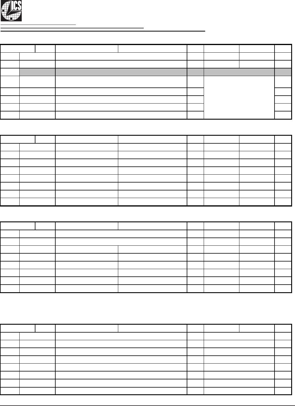
SMBusTable: Gear Ratio Select Register
Pin # Name Control Function T
e0 1PWD
Bit 7
RW Gear Ratio 1:1
1
Bit 6
RW Gear Ratio 1:1
1
Bit 5
RW 1
Bit 4
RW Latch
Bit 3
RW 1
Bit 2
RW 0
Bit 1
RW 1
Bit 0
RW 1
SMBusTable: Output Control Register
Pin # Name Control Function T
e0 1PWD
Bit 7
DIF_7 Output Control RW Hi-Z Enable 1
Bit 6
DIF_6 Output Control RW Hi-Z Enable 1
Bit 5
DIF_5 Output Control RW Hi-Z Enable 1
Bit 4
DIF_4 Output Control RW Hi-Z Enable 1
Bit 3
DIF_3 Output Control RW Hi-Z Enable 1
Bit 2
DIF_2 Output Control RW Hi-Z Enable 1
Bit 1
DIF_1 Output Control RW Hi-Z Enable 1
Bit 0
DIF_0 Output Control RW Hi-Z Enable 1
SMBusTable: Output and PLL BW Control Register
Pin # Name Control Function T
e0 1PWD
Bit 7
RW High BW Low BW
1
Bit 6
RW Bypass PLL
1
Bit 5
DIF_13 Output Control RW Hi-Z Enable 1
Bit 4
DIF_12 Output Control RW Hi-Z Enable 1
Bit 3
DIF_11 Output Control RW Hi-Z Enable 1
Bit 2
DIF_10 Output Control RW Hi-Z Enable 1
Bit 1
DIF_9 Output Control RW Hi-Z Enable 1
Bit 0
DIF_8 Output Control RW Hi-Z Enable 1
Note: Bit 7 is wired OR to the HIGH_BW# input, any 0 selects High BW
Note: Bit 6 is wired OR to the SMB_A2_PLLBYP# input, any 0 selects Fanout Bypass mode
SMBusTable: Output Enable Readback Register
Pin # Name Control Function T
e0 1PWD
Bit 7
R X
Bit 6
R X
Bit 5
R X
Bit 4
R X
Bit 3
R X
Bit 2
R X
Bit 1
R X
Bit 0
R X
72
Readback
Readback - OE5# Input
Readback - OE6# Input
Readback
Readback
Readback - OE8# Input
Readback
Readback
Readback - OE7# Input
Readback - OE9# Input
see note PLL_BW# adjust
see note BYPASS# test mode / PLL
8
B
te 1
-
-
-
-
B
te 0
DIF(14:0)
DIF(18:15)
Gear Ratio FS4 (Inverse of FS_A_410 input!)
-
-
Group of 15 gear ratio enable
Group of 4 gear ratio enable
Reserved
B
te 3
ReadbackReadback - OE_01234# Input
Readback - SMB_A2_PLLBYP# In Readback
Readback - HIGH_BW# In Readback
B
te 2
Gear Ratio FS3
Gear Ratio FS2
Gear Ratio FS1
See ICS9FG1904-1
Programmable Gear
Ratios Table
Gear Ratio FS0

