4
Integrated
Circuit
Systems, Inc.
ICS9FG1904B-1
1255B—08/03/07
CLK_IN
CLK_IN#
DIF(14:0)
CONTROL
LOGIC
HIGH_BW#
SMB_A2_PLLBYP#
SMBDAT
SMBCLK
CKPWRGD/PD#
SPREAD
COMPATIBLE
GEARING PLL
15
IREF
OE(14:5)#,
OE_01234#
11
SMB_A0
SMB_A1
FS_A_410
DIF(18:15)
4
OE_17_18#
OE_15_16#
SPREAD
COMPATIBLE
1:1 PLL
2
ThThe ICS9FG1904-1 follows the Intel DB1900GS Differential Buffer Specification, except for the output groupings and gear
table. The gear table is a blend of the GS and GSO gearing. This buffer provides 19 output clocks for CPU Host Bus, PCI-
Express, or Fully Buffered DIMM applications. The outputs are configured with two groups. Both groups, DIF_(14:0) and
DIF_(18:15) can be equal to or have a gear ratio to the input clock. A differential CPU clock from a CK410B+ main clock
generator, such as the ICS932S421, drives the ICS9FG1904-1. The ICS9FG1904-1 can provide outputs up to 400MHz.
General Description
Block Diagram
Power Groups
VDD GND
3 2 Main PLLs, Analog
11,27,47,63 10,28,46,64 DIF clocks
Description
Pin Number
5
Integrated
Circuit
Systems, Inc.
ICS9FG1904B-1
1255B—08/03/07
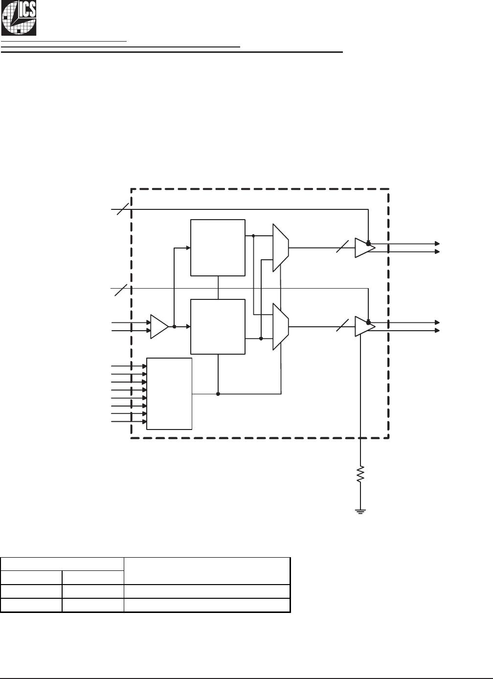
ICS 9FG1904B-1 Programmable Gear Ratios
CLK_IN
(CPU FSB)
MHz
Geared DIF
Outputs
MHz
Mn
Gear
Ratio n/M
(FS_A_410#)
Byte 0,
bit 4
FS4
Byte 0,
bit 3
FS3
Byte 0,
bit 2
FS2
Byte 0,
bit 1
FS1
Byte 0,
bit 0
FS0
Notes
100.00 133.33 3 4 1.333 0 0000
100.00 166.67 3 5 1.667 0 0001
100.00 200.00 1 2 2.000 0 0010
100.00 266.67 3 8 2.667 0 0011
100.00 333.33 3 10 3.333 0 0100
100.00 400.00 1 4 4.000 0 0101
133.33 166.67 4 5 1.250 0 01101
133.33 200.00 2 3 1.500 0 01111
133.33 266.67 1 2 1.250 0 1000
133.33 333.33 2 5 1.500 0 1001
133.33 100.00 4 3 0.750 0 1010
166.67 133.33 5 4 0.800 0 1011
1,3
166.67 200.00 5 6 1.200 0 11001
166.67 266.67 5 8 1.600 0 1101
160/
166.67
320/
333.33
122.000 0 11101,2
166.67 400.00 5 12 2.400 0 1111
200.00 133.33 3 2 0.667 1 00001
200.00 166.67 6 5 0.833 1 00011
200.00 266.67 3 4 1.333 1 00101
200.00 333.33 3 5 1.667 1 00111
200.00 400.00 1 2 2.000 1 01001
266.67 133.33 2 1 0.500 1 01011
266.667/
320.00
166.67/
200.00
850.625 1 01101, 6
266.67 200.00 4 3 0.750 1 01111
333.33 133.33 5 2 0.400 1 10001
320/
333.33
160/
166.67
210.500 1 10011,5
333.33 200.00 5 3 0.600 1 10101
400.00 133.33 3 1 0.333 1 1011
1,4
400.00 160.00 5 2 0.400 1 11001
400.00 166.67 12 5 0.417 1 11011
400.00 320.00 5 4 0.800 1 11101
400.00 333.33 6 5 0.833 1 11111
Notes:
1. Targetted input/output frequency pairs
2. This Gear is also used for 160MHz/320 MHz.
3. Gear Ratio 5/4 is power up default for FS_A_410 = 1
4. Gear Ratio 3/1 is power up default for FS_A_410 = 0
5. This Gear is also used for 400MHz/200MHz
6. This Gear is also used for 320MHz/200MHz
6
Integrated
Circuit
Systems, Inc.
ICS9FG1904B-1
1255B—08/03/07
Byte 9,
bit 2
FSC
Byte9,
bit 1
FSB
Byte 9,
bit 0
FS_A_410
CLK_IN
(CPU FSB)
MHz
1:1 DIF
Outputs
MHz
Notes
101
100.00 100.00 3
001
133.33 133.33 3
011
166.67 166.67
1
010
200.00 200.00 3
000
266.67 266.67 3
100
333.33 333.33 3
110
400.00 400.00
2
111
Notes:FS_A_410 = 1
1. Powerup Default for FS_A_410 = 1
2. Powerup Default for FS_A_410 = 0
3. Setting the exact FSB frequency after Power is required for best phase noise performance.
Reserved
ICS 9FG1904B-1 1:1 PLL Programming
Desired
Decimal
Value
Binary
Value to
write to
Register
20000
30001
50010
70011
40100
60101
10 0110
14 0111
81000
12 1001
20 1010
28 1011
16 1100
24 1101
40 1110
56 1111
Out
p
ut Divider Ratios

9FG1904BK-1LF

Mfr. #:
Manufacturer:
IDT
Description:
Clock Buffer PCIE BUFFER
Lifecycle:
New from this manufacturer.
Delivery:
DHL FedEx Ups TNT EMS
Payment:
T/T Paypal Visa MoneyGram Western Union

Products related to this Datasheet