9
Integrated
Circuit
Systems, Inc.
ICS9FG1904B-1
1255B—08/03/07
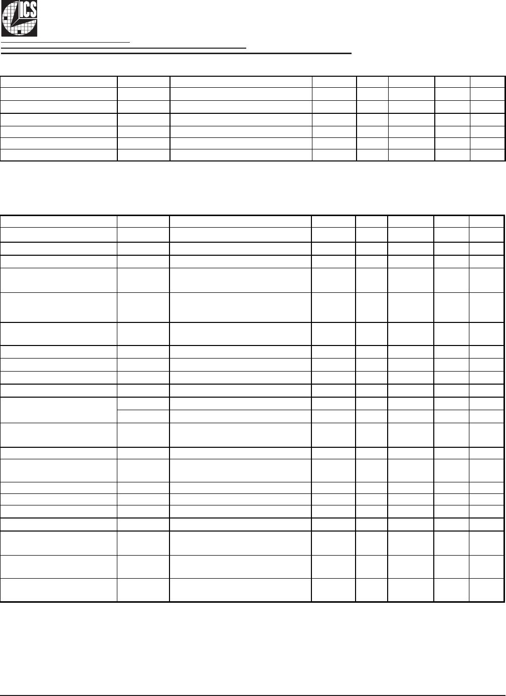
Electrical Characteristics - Skew and Differential Jitter Parameters
T
A
= 0 - 70°C; Supply Voltage V
DD
= 3.3 V +/-5%
Group Parameter Description Min Max Units Notes
CLK_IN, DIF[x:0]
t
SPO_PLL
Input-to-Output Skew in PLL mode (1:1 only),
nominal value @ 25°C, 3.3V
-500 500 ps
1,2,4,5,8
CLK_IN, DIF[x:0]
t
PD_BYP
Input-to-Output Skew in Bypass mode (1:1 only),
nominal value @ 25°C, 3.3V
2.5 4.5 ns
1,2,3,5
CLK_IN, DIF [x:0]
∆
t
SPO_PLL
Input-to-Output Skew Variation in PLL mode
(over specified voltage / temperature operating ranges)
|350| ps
1,2,4,5,6,
10
CLK_IN, DIF [x:0]
∆t
PD_BYP
Input-to-Output Skew Variation in Bypass mode
(over specified voltage / temperature operating ranges)
|500| ps
1,2,3,4,5,
6,10
DIF[14:0]
t
SKEW_G15
Output-to-Output Skew Group of 15
Common to B
ass and PLL mode
100 ps
1,2
DIF[18:15]
tSKEW_G4
Output-to-Output Skew Group of 4 (Common to Bypass and PLL
mode
50 ps
1.2
DIF[18:0]
t
SKEW_A19
Output-to-Output Skew across all 19 outputs
(Common to Bypass and PLL mode - all outputs at same gear)
150 ps
1,2,3
DIF[18:0]
t
JPH
Differential Phase Jitter (RMS Value) 10 ps
1,4,7
DIF[18:0]
t
SSTERROR
Differential Spread Spectrum Tracking Error (peak to peak) 80 ps
1,4,9
NOTES:
8. t is the period of the input clock
10. This parameter is an absolute value. It is not a double-sided figure.
9. Differential spread spectrum tracking error is the difference in spread spectrum tracking between two ICS9FG1900 devices This parameter is measured at
the outputs of two separate ICS9FG1900 devices driven by a single CK410B in Spread Spectrum mode. The ICS9FG1900's must be set to high bandwidth.
The spread spectrum characteristics are: maximum of 0.5%, 30-33KHz modulation frequency, linear profile.
5. Measured with scope averaging on to find mean value.
6. Long-term variation from nominal of input-to-output skew over temperature and voltage for a single device.
7. This parameter is measured at the outputs of two separate ICS9FG1900 devices driven by a single CK410B. The ICS9FG1900's must be set to high
bandwidth. Differential phase jitter is the accumulation of the phase jitter not shared by the outputs (eg. not including the affects of spread spectrum). Target
ran
es of consideration are a
ents with BW of 1-22Mhz and 11-33Mhz.
1. Measured into fixed 2 pF load cap. Input to output skew is measured at the first output edge following the corresponding input.
2. Measured from differential cross-point to differential cross-point
3. All Bypass Mode Input-to-Output specs refer to the timing between an input edge and the specific output edge created by it.
4. This parameter is deterministic for a given device
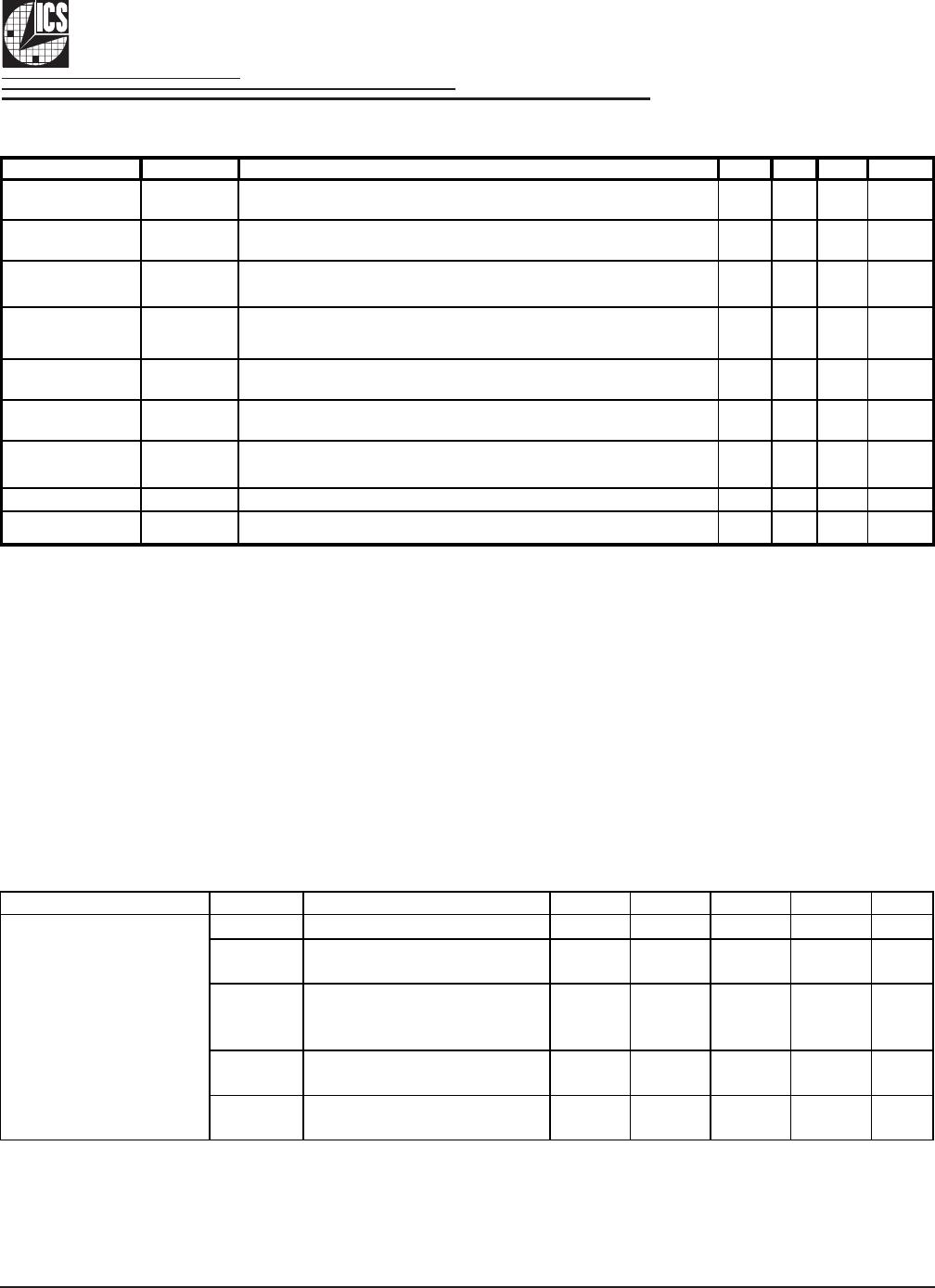
Electrical Characteristics - Phase Jitter Parameters
TA = 0 - 70°C; Supply Voltage VDD = 3.3 V +/-5%, when driven by 932S421B or equivalent
PARAMETER S
mbol Conditions Min T
Ma
Units Notes
t
hPCIe1
PCIe Gen 1 108 ps (p-p) 1,2
t
jphPCIe2Lo
PCIe Gen 2
10kHz < f < 1.5MHz
3ps (RMS)1,2
t
jphPCIe2Hi
PCIe Gen 2
1.5MHz < f < Nyquist (50MHz)
3.1 ps (RMS) 1,2
t
jphFBD1_3.2G
FBD1 3.2/4G
11MHz to 33MHz
3ps (RMS)1,2
t
jphFBD1_4.0G
FBD1 4.8G
11MHz to 33MHz
2.5 ps (RMS) 1,2
Notes:
1
Guaranteed b
desi
n and characterization, not 100% tested in production.
Jitter, Phase
2
See http://www.pcisig.com for complete specs