AD7845
REV. B –9–
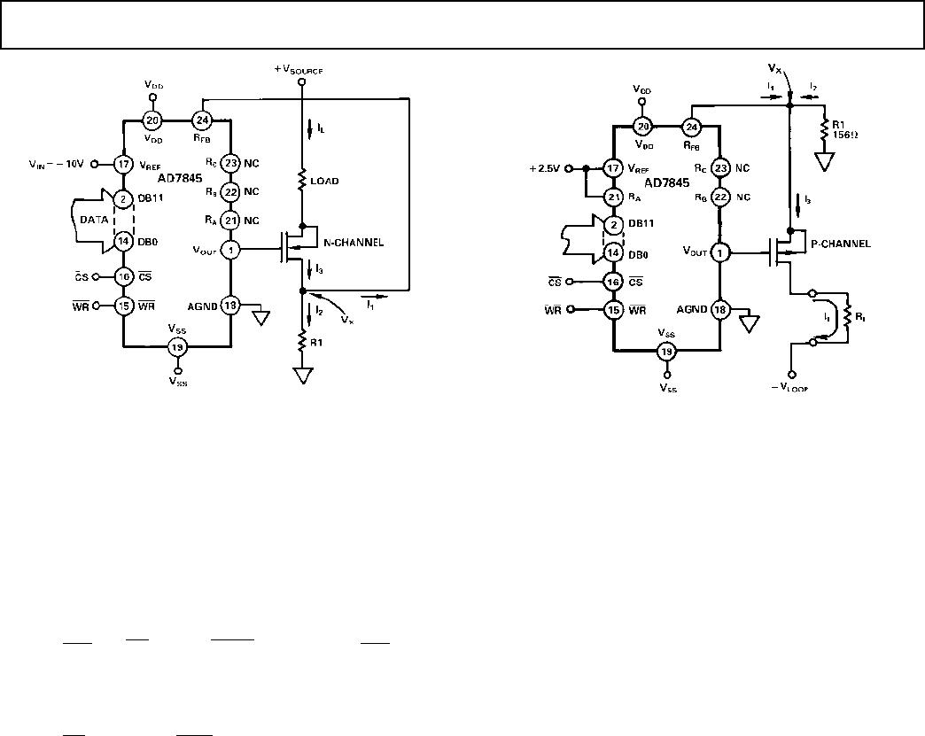
Figure 17. Programmable Current Sink
4–20 mA CURRENT LOOP
The AD7845 provides an excellent way of making a 4-20 mA
current loop circuit. This is basically a variation of the circuits
in Figures 16 and 17 and is shown in Figure 18. The application
resistor R
A
(Value 4R) produces the effective 4 mA offset.
I
L
= I
3
= I
2
+ I
1
Since I
2
> I
1
,
I
L
= –
V
X
156
=
2.5
4R
× R
FB
+
2.5
R
DAC
× D × R
FB
×
1
156
and since R
DAC
=R
FB
=R
I
L
=
2.5
4
+ D ×2.5
×
1000
156
mA
= [4 + (16 × D)]mA, where D goes from 0 to 1 with
Digital Code
When D = 0 (Code of all 0s):
I
L
= 4 mA
When D = 1 (Code of all 1s):
I
L
= 20 mA
The above circuit succeeds in significantly reducing the circuit
component count. Both the on-chip output amplifier and the
application resistor R
A
contribute to this.
Figure 18. 4–20 mA Current Loop
APPLICATION HINTS
General Ground Management: AC or transient voltages
between AGND and DGND can cause noise injection into the
analog output. The simplest method of ensuring that voltages at
AGND and DGND are equal is to tie AGND and DGND
together at the AD7845. In more complex systems where the
AGND and DGND intertie is on the backplane, it is recom-
mended that two diodes be connected in inverse parallel be-
tween the AD7845 AGND and DGND pins (IN914 or
equivalent).
Digital Glitches: When a new digital word is written into the
DAC, it results in a change of voltage applied to some of the
DAC switch gates. This voltage change is coupled across the
switch stray capacitance and appears as an impulse on the cur-
rent output bus of the DAC. In the AD7845, impulses on this
bus are converted to a voltage by R
FB
and the output amplifier.
The output voltage glitch energy is specified as the area of the
resulting spike in nV-seconds. It is measured with V
REF
con-
nected to analog ground and for a zero to full-scale input code
transition. Since microprocessor based systems generally have
noisy grounds which couple into the power supplies, the
AD7845 V
DD
and V
SS
terminals should be decoupled to signal
ground.
Temperature Coefficients: The gain temperature coefficient
of the AD7845 has a maximum value of 5 ppm/°C. This corre-
sponds to worst case gain shift of 2 LSBs over a 100°C tem-
perature range. When trim resistors R1 and R2 in Figure 13
are used to adjust full-scale range, the temperature coefficient
of R1 and R2 must be taken into account. The offset tempera-
ture coefficient is 5 ppm of FSR/°C maximum. This corre-
sponds to a worst case offset shift of 2 LSBs over a 100°C
temperature range.
The reader is referred to Analog Devices Application Note
“Gain Error and Gain Temperature Coefficient of CMOS Mul-
tiplying DACs,” Publication Number E630C-5-3/86.

