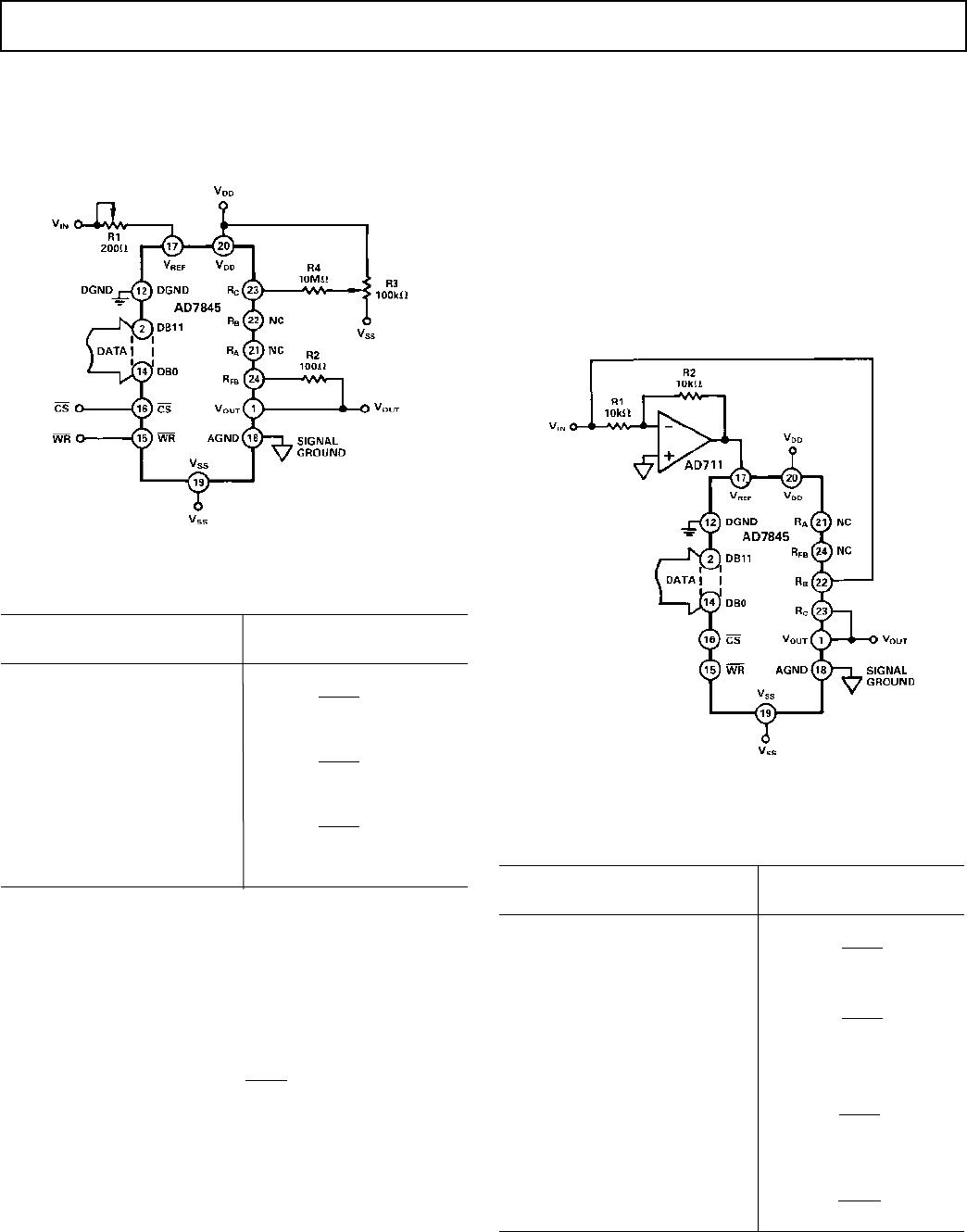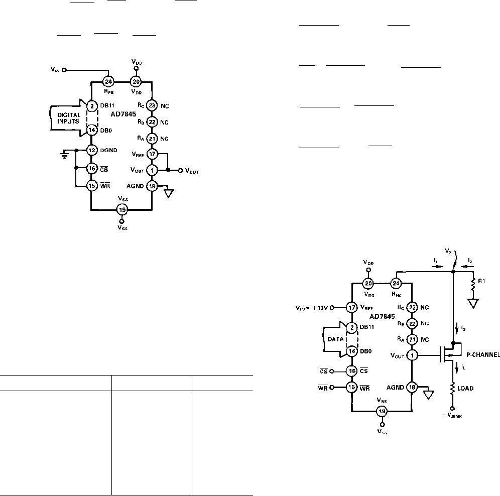
AD7845
REV. B
–6–
PIN FUNCTION DESCRIPTION (DIP)
Pin Mnemonic Description
1V
OUT
Voltage Output Terminal
2-11 DB11–DB2 Data Bit 11 (MSB) to Data Bit 2
12 DGND Digital Ground. The metal lid on the ceramic package is connected to this pin
13-14 DB1–DB0 Data Bit 1 to Data Bit 0 (LSB)
15 WR Write Input. Active low
16 CS Chip Select Input. Active low
17 V
REF
Reference Input Voltage which can be an ac or dc signal
18 AGND Analog Ground. This is the reference point for external analog circuitry
19 V
SS
Negative power supply for the output amplifier (nominal –12 V to +15 V)
20 V
DD
Positive power supply (nominal +12 V to +15 V)
21 R
A
Application resistor. R
A
= 4 R
FB
22 R
B
Application resistor. R
B
= 2 R
FB
23 R
C
Application resistor. R
C
= 2 R
FB
24 R
FB
Feedback resistor in the DAC. For normal operation this is connected to V
OUT
CIRCUIT INFORMATION
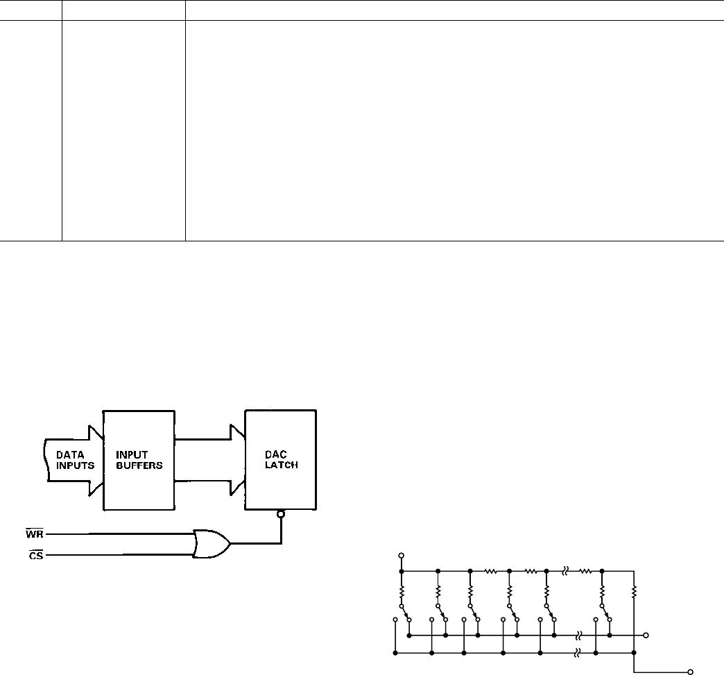
Digital Section
Figure 11 is a simplified circuit diagram of the AD7845 input
control logic. When CS and WR are both low, the DAC latch is
loaded with the data on the data inputs. All the digital inputs
are TTL, HCMOS and +5 V CMOS compatible, facilitating
easy microprocessor interfacing. All digital inputs incorporate
standard protection circuitry.
Figure 11. AD7845 Input Control Logic
D/A Section
Figure 12 shows a simplified circuit diagram for the AD7845
D/A section and output amplifier.
A segmented scheme is used whereby the 2 MSBs of the 12-bit
data word are decoded to drive the three switches A-C. The
remaining 10 bits drive the switches (S0–S9) in a standard R-2R
ladder configuration.
RRR
2R
2R
2R
2R 2R
BA S9
2R
C
V
REF
S8 S0
SHOWN FOR ALL 1s ON DAC
2R
I
OUT
AGND
Figure 12. Simplified Circuit Diagram for the AD7845 D/A
Section
Each of the switches A–C steers 1/4 of the total reference cur-
rent with the remaining 1/4 passing through the R-2R section.
An output amplifier and feedback resistor perform the current-
to-voltage conversion giving
V
OUT
= – D × V
REF
where D is the fractional representation of the digital word. (D
can be set from 0 to 4095/4096.)
The amplifier can maintain ±10 V across a 2 kΩ load. It is inter-
nally compensated and settles to 0.01% FSR (1/2 LSB) in less
than 5 µs. The input offset voltage is laser trimmed at wafer
level. The amplifier slew rate is typically 11 V/µs, and the unity
gain small signal bandwidth is 600 kHz. There are three extra
on-chip resistors (R
A
, R
B
, R
C
) connected to the amplifier invert-
ing terminal. These are useful in a number of applications in-
cluding offset adjustment and gain ranging.