AD7845
REV. B –3–
Limit at T
MIN
to T
MAX
Parameter (All Versions) Units Test Conditions/Comments
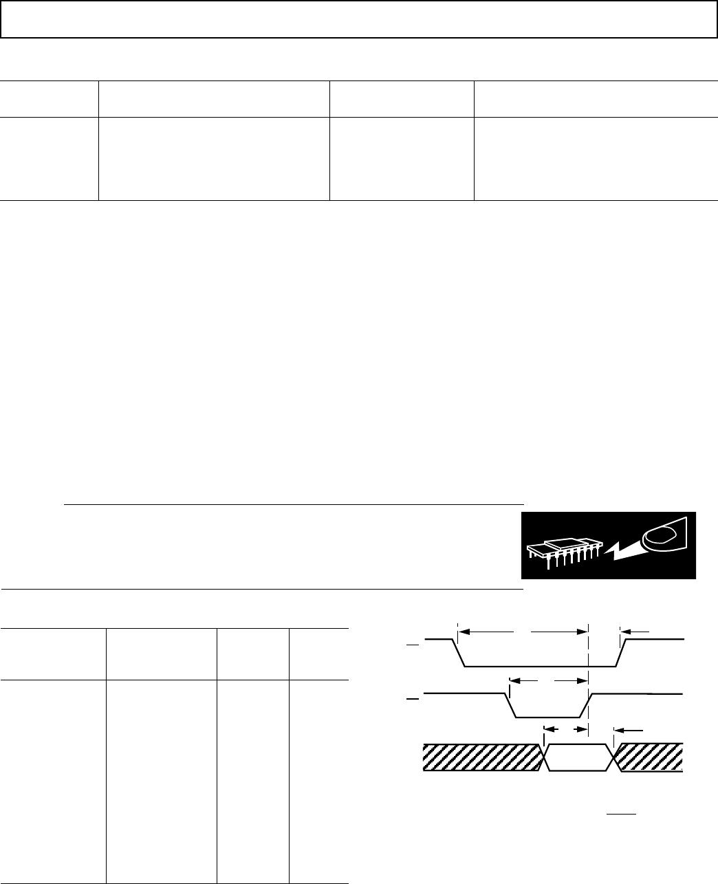
t
CS
30 ns min Chip Select to Write Setup Time
t
CH
0 ns min Chip Select to Write Hold Time
t
WR
30 ns min Write Pulsewidth
t
DS
80 ns min Data Setup Time
t
DH
0 ns min Data Hold Time
NOTES
1
Guaranteed by design and characterization, not production tested.
Specifications subject to change without notice.
TIMING CHARACTERISTICS
1
(V
DD
= +15 V, ⴞ 5%. V
SS
= –15 V, ⴞ 5%. V
REF
= +10 V. AGND = DGND = O V.)
ORDERING GUIDE
1
Relative
Temperature Accuracy Package
Model
2
Range @ +25ⴗC Option
3
AD7845JN 0°C to +70°C ±1 LSB N-24
AD7845KN 0°C to +70°C ±1/2 LSB N-24
AD7845JP 0°C to +70°C ±1 LSB P-28A
AD7845KP 0°C to +70°C ±1/2 LSB P-28A
AD7845JR 0°C to +70°C ±1 LSB R-24
AD7845KR 0°C to +70°C ±1/2 LSB R-24
AD7845AQ –40°C to +85°C ±1 LSB Q-24
AD7845BQ –40°C to +85°C ±1/2 LSB Q-24
AD7845AR –40°C to +85°C ±1 LSB R-24
AD7845BR –40°C to +85°C ±1/2 LSB R-24
AD7845SQ/883B –55°C to +125°C ±1 LSB Q-24
AD7845TQ/883B –55°C to +125°C ±1/2 LSB Q-24
AD7845SE/883B –55°C to +125°C ±1 LSB E-28A
NOTES
1
Analog Devices reserves the right to ship either ceramic (D-24A) or cerdip
(Q-24) hermetic packages.
2
To order MIL-STD-883, Class B processed parts, add /883B to part number.
3
E = Leadless Ceramic Chip Carrier; N = Plastic DIP; P = Plastic Leaded Chip
Carrier; Q = Cerdip; R = SOIC.
CAUTION
ESD (electrostatic discharge) sensitive device. Electrostatic charges as high as 4000 V readily
accumulate on the human body and test equipment and can discharge without detection.
Although the AD7845 features proprietary ESD protection circuitry, permanent damage may
occur on devices subjected to high energy electrostatic discharges. Therefore, proper ESD
precautions are recommended to avoid performance degradation or loss of functionality.
Operating Temperature Range
Commercial (J, K Versions) . . . . . . . . . . . . . 0°C to +70°C
Industrial (A, B Versions) . . . . . . . . . . . . –40°C to +85°C
Extended (S, T Versions) . . . . . . . . . . . . –55°C to +125°C
Storage Temperature Range . . . . . . . . . . . –65°C to +150°C
Lead Temperature (Soldering, 10 sec) . . . . . . . . . . . +300°C
NOTES
1
Stresses above those listed under Absolute Maximum Ratings may cause
permanent damage to the device. This is a stress rating only; functional
operation of the device at these or any other conditions above those indicated in
the operational sections of this specification is not implied. Exposure to absolute
maximum rating conditions for extended periods of time may affect device
reliability. Only one Absolute Maximum Rating may be applied at any one time.
2
V
OUT
may be shorted to AGND provided that the power dissipation of the
package is not exceeded.
CS
WR
DATA
5V
0V
5V
0V
5V
0V
NOTES
1. ALL INPUT SIGNAL RISE AND FALL TIMES MEASURED FROM
10% TO 90% OF +5V. t
R
= t
F
= 20ns.
2. TIMING MEASUREMENT REFERENCE LEVEL IS
V
IH
+ V
IL
2
t
CS
t
CH
t
WR
t
DS
t
DH
Figure 1. AD7845 Timing Diagram
ABSOLUTE MAXIMUM RATINGS
1
(T
A
= +25°C unless otherwise stated)
V
DD
to DGND . . . . . . . . . . . . . . . . . . . . . . . .–0.3 V to +17 V
V
SS
to DGND . . . . . . . . . . . . . . . . . . . . . . . .+0.3 V to –17 V
V
REF
to AGND . . . . . . . . . . . . . . . . V
DD
+ 0.3 V, V
SS
– 0.3 V
V
RFB
to AGND . . . . . . . . . . . . . . . . V
DD
+ 0.3 V, V
SS
– 0.3 V
V
RA
to AGND . . . . . . . . . . . . . . . . . V
DD
+ 0.3 V, V
SS
– 0.3 V
V
RB
to AGND . . . . . . . . . . . . . . . . . V
DD
+ 0.3 V, V
SS
– 0.3 V
V
RC
to AGND . . . . . . . . . . . . . . . . . V
DD
+ 0.3 V, V
SS
– 0.3 V
V
OUT
to AGND
2
. . . . . . . . . . . . . . . V
DD
+ 0.3 V, V
SS
– 0.3 V
AGND to DGND . . . . . . . . . . . . . . . . . . . . . . . . –0.3 V, V
DD
Digital Input Voltage to DGND . . . . . –0.3 V to V
DD
+ 0.3 V
Power Dissipation (Any Package)
To +75°C . . . . . . . . . . . . . . . . . . . . . . . . . . . . . . 650 mW
Derates above +75°C . . . . . . . . . . . . . . . . . . . . . 10 mW/°C
WARNING!
ESD SENSITIVE DEVICE

