AD8182ARZ-RL

REV. B
Information furnished by Analog Devices is believed to be accurate and
reliable. However, no responsibility is assumed by Analog Devices for its
use, nor for any infringements of patents or other rights of third parties
which may result from its use. No license is granted by implication or
otherwise under any patent or patent rights of Analog Devices.
a
750 MHz, 3.8 mA
10 ns Switching Multiplexers
AD8180/AD8182
FUNCTIONAL BLOCK DIAGRAM
1
2
3
4
8
7
6
5
AD8180
IN0
–V
S
OUT
ENABLE
SELECT
GND
IN1
+V
S
DECODER
+1
+1
1
2
3
4
14
13
12
11
AD8182
–V
S
OUT A
ENABLE A
SELECT A
5
6
7
10
9
8
SELECT B
OUT B
ENABLE B
DECODER
+1
+1
DECODER
+1
+1
IN0 A
GND
IN1 A
+V
S
IN1 B
GND
IN0 B
FEATURES
Fully Buffered Inputs and Outputs
Fast Channel Switching: 10 ns
High Speed
> 750 MHz Bandwidth (–3 dB)
750 V/s Slew Rate
Fast Settling Time of 14 ns to 0.1%
Low Power: 3.8 mA (AD8180), 6.8 mA (AD8182)
Excellent Video Specifications (R
L
1 k)
Gain Flatness of 0.1 dB Beyond 100 MHz
0.02% Differential Gain Error
0.02 Differential Phase Error
Low Glitch: < 35 mV
Low All-Hostile Crosstalk of –80 dB @ 5 MHz
High “OFF” Isolation of –90 dB @ 5 MHz
Low Cost
Fast Output Disable Feature for Connecting Multiple Devices
APPLICATIONS
Pixel Switching for “Picture-In-Picture”
Switching in LCD and Plasma Displays
Video Switchers and Routers
PRODUCT DESCRIPTION
The AD8180 (single) and AD8182 (dual) are high speed 2-to-1
multiplexers. They offer –3 dB signal bandwidth greater than
750 MHz along with slew rate of 750 V/µs. With better than
80 dB of crosstalk and isolation, they are useful in many high
speed applications. The differential gain and differential phase
error of 0.02% and 0.02°, along with 0.1 dB flatness beyond
100 MHz make the AD8180 and AD8182 ideal for professional
video multiplexing. They offer 10 ns switching time making
them an excellent choice for pixel switching (picture-in-picture)
while consuming less than 3.8 mA (per 2:1 mux) on ±5 V sup-
ply voltages.
Both devices offer a high speed disable feature allowing the
output to be configured into a high impedance state. This al-
lows multiple outputs to be connected together for cascading
stages while the “OFF” channels do not load the output bus.
They operate on voltage supplies of ±5 V and are offered in 8-
and 14-lead plastic DIP and SOIC packages.
500mV
/DIV
5ns/DIV
Figure 1. AD8180/AD8182 Switching Characteristics
Table I. Truth Table
SELECT ENABLE OUTPUT
00 IN0
10 IN1
0 1 High Z
1 1 High Z
One Technology Way, P.O. Box 9106, Norwood, MA 02062-9106, U.S.A.
Tel: 781/329-4700 World Wide Web Site: http://www.analog.com
Fax: 781/326-8703 © Analog Devices, Inc., 2000
REV. B–2–
AD8180/AD8182–SPECIFICATIONS
AD8180A/AD8182A
Parameter Conditions Min Typ Max Units
SWITCHING CHARACTERISTICS
Channel Switching Time
1
Channel-to-Channel
50% Logic to 10% Output Settling IN0 = +1 V, IN1 = –1 V; R
L
= 1 k 5ns
50% Logic to 90% Output Settling IN0 = +1 V, IN1 = –1 V; R
L
= 1 k 10 ns
50% Logic to 99.9% Output Settling IN0 = +1 V, IN1 = –1 V; R
L
= 1 k 14 ns
ENABLE to Channel ON Time
2
SEL = 0 or 1
50% Logic to 90% Output Settling IN0 = +1 V, –1 V or IN1 = –1 V, +1 V; R
L
= 1 k 10.5 ns
ENABLE to Channel OFF Time
2
SEL = 0 or 1
50% Logic to 90% Output Settling IN0 = +1 V, –1 V or IN1 = –1 V, +1 V; R
L
= 1 k 11 ns
Channel Switching Transient (Glitch)
3
All Inputs Are Grounded, R
L
= 1 kΩ±25 /±35 mV
DIGITAL INPUTS
Logic “1” Voltage SEL and ENABLE Inputs 2.0 V
Logic “0” Voltage SEL and ENABLE Inputs 0.8 V
Logic “1” Input Current SEL, ENABLE = +4 V 10 200 nA
Logic “0” Input Current SEL, ENABLE = +0.4 V 2 3 µA
DYNAMIC PERFORMANCE
–3 dB Bandwidth (Small Signal)
4
AD8180R V
IN
= 50 mV rms, R
L
= 5 k 750 930 MHz
–3 dB Bandwidth (Small Signal)
4
AD8182R V
IN
= 50 mV rms, R
L
= 5 k 640 780 MHz
–3 dB Bandwidth (Large Signal) AD8180R V
IN
= 1 V rms, R
L
= 5 k 120 150 MHz
–3 dB Bandwidth (Large Si AD8182R V
IN
= 1 V rms, R
L
= 5 k 110 135 MHz
0.1 dB Bandwidth
4, 5
V
IN
= 50 mV rms, R
L
= 5 k, R
S
= 0 100 MHz
AD8180R V
IN
= 50 mV rms, R
L
= 1 k–5 k, R
S
= 150 210 MHz
0.1 dB Bandwidth
4, 5
AD8182R V
IN
= 50 mV rms, R
L
= 1 k–5 k, R
S
= 125 210 MHz
Slew Rate 2 V Step 750 V/µs
Settling Time to 0.1% 2 V Step 14 ns
DISTORTION/NOISE PERFORMANCE
Differential Gain ƒ = 3.58 MHz, R
L
= 1 k 0.02 0.04 %
Differential Phase ƒ = 3.58 MHz, R
L
= 1 k 0.02 0.04 Degrees
All Hostile Crosstalk
6
AD8180R ƒ = 5 MHz, R
L
= 1 k –80 dB
ƒ = 30 MHz, R
L
= 1 k –65 dB
All Hostile Crosstalk
6
AD8182R ƒ = 5 MHz, R
L
= 1 k –78 dB
ƒ = 30 MHz, R
L
= 1 k –63 dB
OFF Isolation
7
AD8180R ƒ = 5 MHz, R
L
= 30 –89 dB
OFF Isolation
7
AD8182R ƒ = 5 MHz, R
L
= 30 –93 dB
Voltage Noise ƒ = 10 kHz–30 MHz 4.5 nV/Hz
Total Harmonic Distortion ƒ
C
= 10 MHz, V
O
= 2 V p-p, R
L
= 1 k –78 dBc
DC/TRANSFER CHARACTERISTICS
Voltage Gain
8
V
IN
= ±1 V, R
L
= 2 k 0.982 V/V
V
IN
= ±1 V, R
L
= 10 k 0.986 0.993 V/V
Input Offset Voltage 112mV
T
MIN
to T
MAX
15 mV
Input Offset Voltage Matching Channel-to-Channel 0.5 4 mV
Input Offset Drift 11 µV/°C
Input Bias Current 15 µA
T
MIN
to T
MAX
7 µA
Input Bias Current Drift 12 nA/°C
INPUT CHARACTERISTICS
Input Resistance 1 2.2 M
Input Capacitance Channel Enabled (R Package) 1.5 pF
Channel Disabled (R Package) 1.5 pF
Input Voltage Range ±3.3 V
OUTPUT CHARACTERISTICS
Output Voltage Swing R
L
= 500
9
±3.0 ±3.1 V
Short Circuit Current 30 mA
Output Resistance Enabled 27
Disabled 1 10 M
Output Capacitance Disabled (R Package) 1.7 pF
POWER SUPPLY
Operating Range ±4 ±6V
Power Supply Rejection Ratio +PSRR +V
S
= +4.5 V to +5.5 V, –V
S
= –5 V 54 57 dB
Power Supply Rejection Ratio –PSRR –V
S
= –4.5 V to –5.5 V, +V
S
= +5 V 45 51 dB
Quiescent Current All Channels “ON” 3.8/6.8 4.5/8 mA
T
MIN
to T
MAX
4.75/8.5 mA
All Channels “OFF” 1.3/2 2/3 mA
T
MIN
to T
MAX
2/3 mA
AD8182, One Channel “ON” 4 mA
OPERATING TEMPERATURE RANGE –40 +85 °C
(@ T
A
= +25C, V
S
= 5 V, R
L
= 2 k unless otherwise noted)
NOTES
1
ENABLE pin is grounded. IN0 = +1 V dc, IN1 = –1 V dc. SELECT input is driven with 0 V to +5 V pulse. Measure transition time from 50% of the SELECT input value
(+2.5 V) and 10% (or 90%) of the total output voltage transition from IN0 channel voltage (+1 V) to IN1 (–1 V), or vice versa.
2
ENABLE pin is driven with 0 V to +5 V pulse (with 3 ns edges). State of SELECT input determines which channel is activated (i.e., if SELECT = Logic 0, IN0 is selected). Set
IN0 = +1 V dc, IN1 = –1 V dc, and measure transition time from 50% of ENABLE pulse (+2.5 V) to 90% of the total output voltage change. In Figure 5, t
OFF
is the disable
time,
t
ON
is the enable time.
3
All inputs are grounded. SELECT input is driven with 0 V to +5 V pulse. The outputs are monitored. Speeding the edges of the SELECT pulse increases the glitch magnitude
due to coupling via the ground plane. Removing the SELECT input termination will lower glitch, as does increasing R
L
.
4
Decreasing R
L
lowers the bandwidth slightly. Increasing C
L
lowers the bandwidth considerably (see Figure 19).
5
A resistor (R
S
) placed in series with the mux inputs serves to optimize 0.1 dB flatness, but is not required. Increasing output capacitance will increase peaking and reduce band-
width (see Figure 20.)
6
Select input which is not being driven (i.e., if SELECT is Logic 1, input activated is IN1); drive all other inputs with V
IN
= 0.707 V rms and monitor output at ƒ = 5 and 30 MHz.
R
L
= 1 k (see Figure 13).
7
Mux is disabled (i.e., ENABLE = Logic 1) and all inputs are driven simultaneously with V
IN
= 0.446 V rms. Output is monitored at ƒ = 5 and 30 MHz. R
L
= 30 to simulate
R
ON
of one enabled mux within a system (see Figure 14). In this mode the output impedance is very high (typ 10 M), and the signal couples across the package; the load imped-
ance determines the crosstalk.
8
Voltage gain decreases for lower values of R
L
. The resistive divider formed by the mux enabled output resistance (27 ) and R
L
causes a gain which decreases as R
L
decreases
(i.e., the voltage gain is approximately 0.97 V/V (3% gain error) for R
L
= 1 k).
9
Larger values of R
L
provide wider output voltage swings, as well as better gain accuracy. See Note 8.
Specifications subject to change without notice.
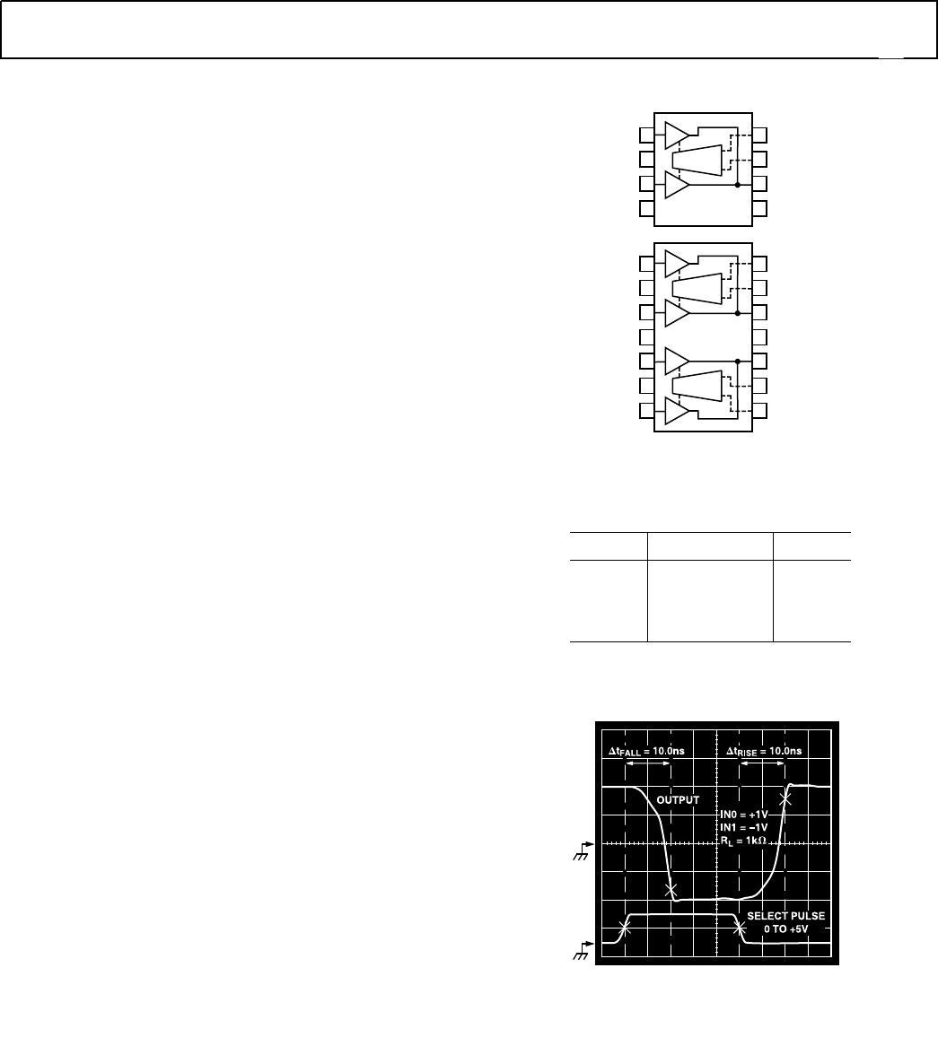
AD8180/AD8182
CAUTION
ESD (electrostatic discharge) sensitive device. Electrostatic charges as high as 4000 V readily
accumulate on the human body and test equipment and can discharge without detection.
Although the AD8180/AD8182 feature proprietary ESD protection circuitry, permanent damage
may occur on devices subjected to high energy electrostatic discharges. Therefore, proper ESD
precautions are recommended to avoid performance degradation or loss of functionality.
–3–
REV. B
ABSOLUTE MAXIMUM RATINGS
1
Supply Voltage . . . . . . . . . . . . . . . . . . . . . . . . . . . . . . . . . 12.6 V
Internal Power Dissipation
2
AD8180 8-Lead Plastic DIP (N) . . . . . . . . . . . . . . . . 1.3 Watts
AD8180 8-Lead Small Outline (R) . . . . . . . . . . . . . . 0.9 Watts
AD8182 14-Lead Plastic DIP (N) . . . . . . . . . . . . . . . 1.6 Watts
AD8182 14-Lead Small Outline (R) . . . . . . . . . . . . . 1.0 Watts
Input Voltage . . . . . . . . . . . . . . . . . . . . . . . . . . . . . . . . . . . . . ±V
S
Output Short Circuit Duration . . . . . Observe Power Derating Curves
Storage Temperature Range
N and R Package . . . . . . . . . . . . . . . . . . . . . . –65°C to +125°C
Lead Temperature Range (Soldering 10 sec) . . . . . . . . . . +300°C
NOTES
1
Stresses above those listed under Absolute Maximum Ratings may cause perma-
nent damage to the device. This is a stress rating only; functional operation of the
device at these or any other conditions above those indicated in the operational
section of this specification is not implied. Exposure to absolute maximum rating
conditions for extended periods may affect device reliability.
2
Specification is for device in free air: 8-Lead Plastic DIP Package: θ
JA
= 90°C/W;
8-Lead SOIC Package: θ
JA
= 155°C/W; 14-Lead Plastic Package: θ
JA
= 75°C/W;
14-Lead SOIC Package: θ
JA
= 120°C/W, where P
D
= (T
J
–T
A
)/θ
JA
.
ORDERING GUIDE
Temperature Package Package
Model Range Description Option
AD8180AN –40°C to +85°C 8-Lead Plastic DIP N-8
AD8180AR –40°C to +85°C 8-Lead SOIC SO-8
AD8180AR-REEL –40°C to +85°C 13" Reel SOIC SO-8
AD8180AR-REEL7 –40°C to +85°C 7" Reel SOIC SO-8
AD8182AN –40°C to +85°C 14-Lead Plastic DIP N-14
AD8182AR –40°C to +85°C 14-Lead Narrow SOIC R-14
AD8182AR-REEL –40°C to +85°C 13" Reel SOIC R-14
AD8182AR-REEL7 –40°C to +85°C 7" Reel SOIC R-14
AD8180-EB Evaluation Board
AD8182-EB Evaluation Board
MAXIMUM POWER DISSIPATION
The maximum power that can be safely dissipated by the
AD8180 and AD8182 is limited by the associated rise in junc-
tion temperature. The maximum safe junction temperature for
plastic encapsulated devices is determined by the glass transition
temperature of the plastic, approximately +150°C. Exceeding
this limit temporarily may cause a shift in parametric perfor-
mance due to a change in the stresses exerted on the die by the
package. Exceeding a junction temperature of +175°C for an
extended period can result in device failure.
While the AD8180 and AD8182 are internally short circuit
protected, this may not be sufficient to guarantee that the maxi-
mum junction temperature (+150°C) is not exceeded under all
conditions. To ensure proper operation, it is necessary to observe
the maximum power derating curves shown in Figures 2 and 3.
MAXIMUM POWER DISSIPATION – Watts
AMBIENT TEMPERATURE – 8C
2.0
1.5
0
–50 90–40 –30 –20 –10 0 10 20 30 50 60 70 8040
1.0
0.5
8-LEAD PLASTIC DIP PACKAGE
8-LEAD SOIC PACKAGE
T
J
= +1508C
Figure 2. AD8180 Maximum Power Dissipation vs.
Temperature
AMBIENT TEMPERATURE – 8C
2.5
2.0
0.5
–50 90–40
MAXIMUM POWER DISSIPATION – Watts
–30 –20 –10 0 10 20 30 40 50 60 80
1.5
1.0
70
14-LEAD SOIC
14-LEAD
PLASTIC DIP PACKAGE
T
J
= +1508C
Figure 3. AD8182 Maximum Power Dissipation vs.
Temperature
WARNING!
ESD SENSITIVE DEVICE

AD8182ARZ-RL

Mfr. #:
Manufacturer:
Analog Devices Inc.
Description:
Multiplexer Switch ICs Dual 2:1 Buffered 750MHz 3.8mA 10ns
Lifecycle:
New from this manufacturer.
Delivery:
DHL FedEx Ups TNT EMS
Payment:
T/T Paypal Visa MoneyGram Western Union