AD8180/AD8182
–10–
REV. B
EVALUATION BOARD
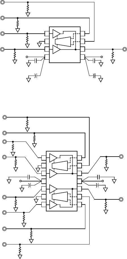
Evaluation boards for the AD8180R and AD8182R are available
which have been carefully laid out and tested to demonstrate the
specified high speed performance of the devices. Figure 26 and
Figure 27 show the schematics of the AD8180 and AD8182
evaluation boards respectively. For ordering information, please
refer to the Ordering Guide.
Because the footprint of the AD8180 fits directly on to that of
the AD8182, one board layout can be used for both devices. In the
case of the AD8180, only the top half of the board is populated.
Figure 28 shows the silkscreen of the component side and Fig-
ure 30 shows the silkscreen of the solder side. Figures 29 and 31
show the layout of the component side and solder side respectively.
The evaluation board is provided with 49.9 Ω termination resis-
tors on all inputs. This is to allow the performance to be evalu-
ated at very high frequencies where 50 Ω termination is most
popular. To use the evaluation board in video applications, the
termination resistors should be replaced with 75 Ω resistors.
The multiplexer outputs are loaded with 4.99 kΩ resistors. In
order to avoid large gain errors, these load resistors should be
greater than or equal to 1 kΩ. For connection to external instru-
ments, oscilloscope scope probe adapters are provided. This
allows direct connection of FET probes to the board. For verifi-
cation of data sheet specifications, use of FET probes with a
bandwidth > 1 GHz is recommended because of their low input
capacitance. The probe adapters used on the board have the
same footprint as SMA, SMB and SMC type connectors allow-
ing easy replacement if necessary.
8
7
6
5
+V
S
C4
10mF
C1
0.1mF
R10
49.9V
1
2
3
4
AD8180R
DECODER
+1
+1
+
R1
49.9V
IN1
IN0
SELECT
R9
49.9V
ENABLE
R8
49.9V
+
–V
S
C3
10mF
C2
0.1mF
R7
4.99kV
OUT
(SCOPE PROBE
ADAPTER)
UNLESS OTHERWISE NOTED, CONNECTORS ARE SMA TYPE
Figure 26. AD8180R Evaluation Board
–V
S
+
+V
S
C1
0.1mF
C4
10mF
R10
49.9V
1
2
3
4
14
13
12
11
AD8182R
5
6
7
10
9
8
DECODER
+1
+1
DECODER
+1
+1
R1
49.9V
IN1 A
IN0 A
R9
49.9V
SELECT A
R8
49.9V
ENABLE A
R2
49.9V
IN1 B
IN0 B
R3
49.9V
R4
49.9V
SELECT B
R5
49.9V
ENABLE B
+
C3
10mF
C2
0.1mF
OUTB
(SCOPE PROBE
ADAPTER)
OUTA
(SCOPE PROBE
ADAPTER)
R6
4.99kV
R7
4.99kV
UNLESS OTHERWISE NOTED, CONNECTORS ARE SMA TYPE
Figure 27. AD8182R Evaluation Board

