PCA9536 All information provided in this document is subject to legal disclaimers. © NXP Semiconductors N.V. 2017. All rights reserved.
Product data sheet Rev. 6 — 7 November 2017 13 of 24
NXP Semiconductors
PCA9536
4-bit I
2
C-bus and SMBus I/O port
10. Dynamic characteristics
[1] t
VD;ACK
= time for Acknowledgement signal from SCL LOW to SDA (out) LOW.
[2] t
VD;DAT
= minimum time for SDA data output to be valid following SCL LOW.
[3] C
b
= total capacitance of one bus line in pF.
Table 11. Dynamic characteristics
Symbol Parameter Conditions Standard-mode
I
2
C-bus
Fast-mode I
2
C-bus Unit
Min Max Min Max
f
SCL
SCL clock frequency 0 100 0 400 kHz
t
BUF
bus free time between a STOP and
START condition
4.7 - 1.3 - s
t
HD;STA
hold time (repeated) START condition 4.0 - 0.6 - s
t
SU;STA
set-up time for a repeated START
condition
4.7 - 0.6 - s
t
SU;STO
set-up time for STOP condition 4.0 - 0.6 - s
t
HD;DAT
data hold time 0 - 0 - s
t
VD;ACK
data valid acknowledge time
[1]
0.3 3.45 0.1 0.9 s
t
VD;DAT
data valid time
[2]
300 - 50 - ns
t
SU;DAT
data set-up time 250 - 100 - ns
t
LOW
LOW period of the SCL clock 4.7 - 1.3 - s
t
HIGH
HIGH period of the SCL clock 4.0 - 0.6 - s
t
r
rise time of both SDA and SCL signals - 1000 20 + 0.1C
b
[3]
300 ns
t
f
fall time of both SDA and SCL signals - 300 20 + 0.1C
b
[3]
300 ns
t
SP
pulse width of spikes that must be
suppressed by the input filter
- 50 - 50 ns
Port timing
t
v(Q)
data output valid time - 200 - 200 ns
t
su(D)
data input set-up time 100 - 100 - ns
t
h(D)
data input hold time 1 - 1 - s
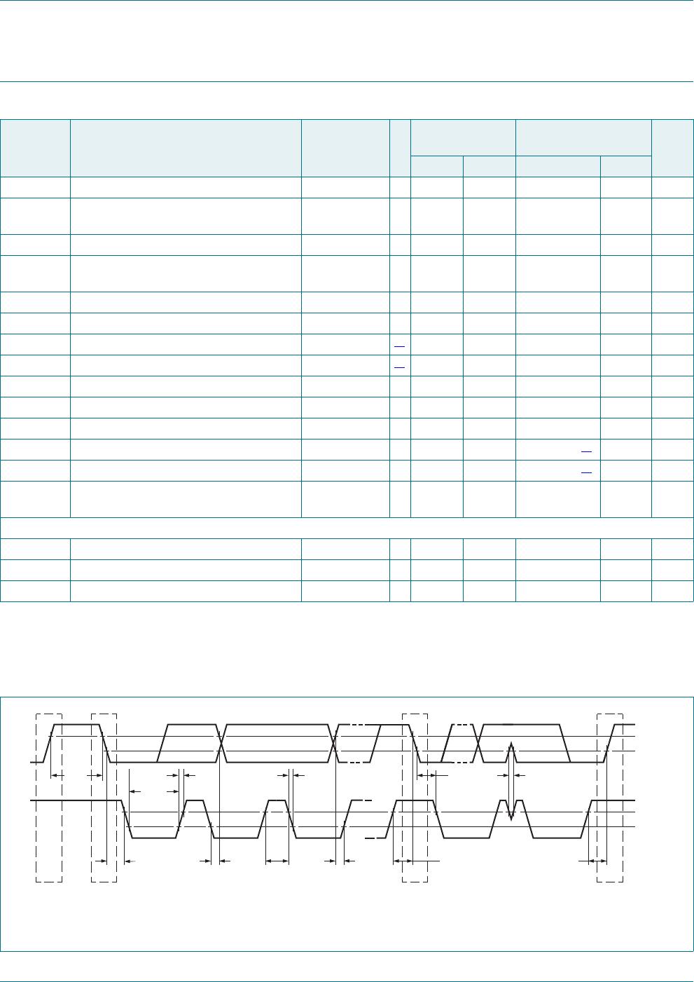
Fig 12. Definition of timing
t
SP
t
BUF
t
HD;STA
PP S
t
LOW
t
r
t
HD;DAT
t
f
t
HIGH
t
SU;DAT
t
SU;STA
Sr
t
HD;STA
t
SU;STO
SDA
SCL
002aaa986
0.7 × V
DD
0.3 × V
DD
0.7 × V
DD
0.3 × V
DD
PCA9536 All information provided in this document is subject to legal disclaimers. © NXP Semiconductors N.V. 2017. All rights reserved.
Product data sheet Rev. 6 — 7 November 2017 14 of 24
NXP Semiconductors
PCA9536
4-bit I
2
C-bus and SMBus I/O port
11. Test information
Rise and fall times refer to V
IL
and V
IH
Fig 13. I
2
C-bus timing diagram
002aab175
protocol
START
condition
(S)
bit 7
MSB
(A7)
bit 6
(A6)
bit 0
(R/W)
acknowledge
(A)
STOP
condition
(P)
SCL
SDA
t
HD;STA
t
SU;DAT
t
HD;DAT
t
f
t
BUF
t
SU;STA
t
LOW
t
HIGH
t
VD;ACK
t
SU;STO
1
/ f
SCL
t
r
t
VD;DAT
0.3 × V
DD
0.7 × V
DD
0.3 × V
DD
0.7 × V
DD
R
L
= load resistor.
C
L
= load capacitance includes jig and probe capacitance.
R
T
= termination resistance should be equal to the output impedance Z
o
of the pulse generators.
Fig 14. Test circuitry for switching times
Fig 15. Test circuit
Table 12. Test data
Test Load Switch
C
L
R
L
t
v(Q)
50 pF 500 2V
DD
PULSE
GENERATOR
V
O
C
L
50 pF
R
L
500 Ω
002aab880
R
T
V
I
V
DD
DUT
V
DD
open
V
SS
C
L
50 pF
500 Ω
002aab881
2V
DD
open
V
SS
S1
from output
under test
500 Ω
PCA9536 All information provided in this document is subject to legal disclaimers. © NXP Semiconductors N.V. 2017. All rights reserved.
Product data sheet Rev. 6 — 7 November 2017 15 of 24
NXP Semiconductors
PCA9536
4-bit I
2
C-bus and SMBus I/O port
12. Package outline
Fig 16. Package outline SOT96-1 (SO8)
UNIT
A
max.
A
1
A
2
A
3
b
p
cD
(1)
E
(2)
(1)
eH
E
LL
p
QZywv θ
REFERENCES
OUTLINE
VERSION
EUROPEAN
PROJECTION
ISSUE DATE
IEC JEDEC JEITA
mm
inches
1.75
0.25
0.10
1.45
1.25
0.25
0.49
0.36
0.25
0.19
5.0
4.8
4.0
3.8
1.27
6.2
5.8
1.05
0.7
0.6
0.7
0.3
8
0
o
o
0.25 0.10.25
DIMENSIONS (inch dimensions are derived from the original mm dimensions)
Notes
1. Plastic or metal protrusions of 0.15 mm (0.006 inch) maximum per side are not included.
2. Plastic or metal protrusions of 0.25 mm (0.01 inch) maximum per side are not included.
1.0
0.4
SOT96-1
X
w M
θ
A
A
1
A
2
b
p
D
H
E
L
p
Q
detail X
E
Z
e
c
L
v M
A
(A )
3
A
4
5
pin 1 index
1
8
y
076E03 MS-012
0.069
0.010
0.004
0.057
0.049
0.01
0.019
0.014
0.0100
0.0075
0.20
0.19
0.16
0.15
0.05
0.244
0.228
0.028
0.024
0.028
0.012
0.010.010.041 0.004
0.039
0.016
0 2.5 5 mm
scale
SO8: plastic small outline package; 8 leads; body width 3.9 mm
SOT96-1
99-12-27
03-02-18

PCA9536DP,118

Mfr. #:
Manufacturer:
NXP Semiconductors
Description:
Interface - I/O Expanders I2C/SMBUS 4BIT GPIO
Lifecycle:
New from this manufacturer.
Delivery:
DHL FedEx Ups TNT EMS
Payment:
T/T Paypal Visa MoneyGram Western Union