PCA9536 All information provided in this document is subject to legal disclaimers. © NXP Semiconductors N.V. 2017. All rights reserved.
Product data sheet Rev. 6 — 7 November 2017 7 of 24
NXP Semiconductors
PCA9536
4-bit I
2
C-bus and SMBus I/O port
6.1.5 Register 3 - Configuration register
This register configures the directions of the I/O pins. If a bit in this register is set, the
corresponding port pin is enabled as an input with high-impedance output driver. If a bit in
this register is cleared, the corresponding port pin is enabled as an output. At reset, the
I/Os are configured as inputs with a weak pull-up to V
DD
.
‘Not used’ bits can be programmed with either logic 0 or logic 1.
6.2 Power-on reset
When power is applied to V
DD
, an internal Power-On Reset (POR) holds the PCA9536 in
a reset condition until V
DD
has reached V
POR
. At that point, the reset condition is released
and the PCA9536 registers and state machine will initialize to their default states.
Thereafter, V
DD
must be lowered below 0.2 V to reset the device.
For a power reset cycle, V
DD
must be lowered below 0.2 V and then restored to the
operating voltage.
6.3 I/O port
When an I/O is configured as an input, FETs Q1 and Q2 are off, creating a
high-impedance input with a weak pull-up (100 k typical) to V
DD
. The input voltage may
be raised above V
DD
to a maximum of 5.5 V.
If the I/O is configured as an output, then either Q1 or Q2 is enabled, depending on the
state of the Output Port register. Care should be exercised if an external voltage is applied
to an I/O configured as an output because of the low-impedance paths that exist between
the pin and either V
DD
or V
SS
.
Table 8. Register 3 - Configuration register bit description
Legend: * default value
Bit Symbol Access Value Description
7 C7 R/W 1* not used
6C6 R/W 1*
5C5 R/W 1*
4C4 R/W 1*
3 C3 R/W 1* configures the directions of the I/O pins
0 = corresponding port pin enabled as an output
1 = corresponding port pin configured as input
(default value)
2C2 R/W 1*
1C1 R/W 1*
0C0 R/W 1*
PCA9536 All information provided in this document is subject to legal disclaimers. © NXP Semiconductors N.V. 2017. All rights reserved.
Product data sheet Rev. 6 — 7 November 2017 8 of 24
NXP Semiconductors
PCA9536
4-bit I
2
C-bus and SMBus I/O port
6.4 Device address
6.5 Bus transactions
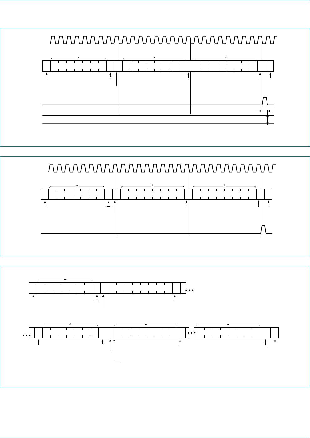
Data is transmitted to the PCA9536 registers using the Write mode as shown in Figure 7
and Figure 8
. Data is read from the PCA9536 registers using the Read mode as shown in
Figure 9
and Figure 10. These devices do not implement an auto-increment function, so
once a command byte has been sent, the register which was addressed will continue to
be accessed by reads until a new command byte has been sent.
Remark: At power-on reset, all registers return to default values.
Fig 5. Simplified schematic of IO0 to IO3
V
DD
IO0 to IO3
output port
register data
configuration
register
DQ
CK Q
data from
shift register
write configuration
pulse
output port
register
DQ
CK
write pulse
polarity inversion
register
DQ
CK
data from
shift register
write polarity
pulse
input port
register
DQ
CK
read pulse
input port
register data
polarity inversion
register data
002aab852
FF
data from
shift register
FF
FF
FF
Q1
100 kΩ
Q2
V
SS
Fig 6. PCA9536 device address
R/W
002aab853
1 0 0 0 0 0 1
fixed
slave address
PCA9536 All information provided in this document is subject to legal disclaimers. © NXP Semiconductors N.V. 2017. All rights reserved.
Product data sheet Rev. 6 — 7 November 2017 9 of 24
NXP Semiconductors
PCA9536
4-bit I
2
C-bus and SMBus I/O port
Fig 7. Write to Output Port register
Fig 8. Write to Configuration register or Polarity Inversion register
0000010AS1
START condition R/W
acknowledge
from slave
002aab855
A
acknowledge
from slave
SCL
SDA
A
data to
register
P
987654321
command byte
acknowledge
from slave
data to register
DATA
slave address
0000001/00
STOP
condition
Fig 9. Read from register
0000010AS1
START condition R/W
acknowledge
from slave
002aab856
A
acknowledge
from slave
SDA
A P
command byte
acknowledge
from master
data from register
DATA (first byte)
slave address
STOP
condition
S
(repeated)
START condition
(cont.)
(cont.)
0000011A1
R/W
acknowledge
from slave
slave address
at this moment master-transmitter becomes master-receiver
and slave-receiver becomes slave-transmitter
NA
no acknowledge
from master
data from register
DATA (last byte)

PCA9536DP,118

Mfr. #:
Manufacturer:
NXP Semiconductors
Description:
Interface - I/O Expanders I2C/SMBUS 4BIT GPIO
Lifecycle:
New from this manufacturer.
Delivery:
DHL FedEx Ups TNT EMS
Payment:
T/T Paypal Visa MoneyGram Western Union