12
LTC1405
1405fa
Differential Operation
The THD and SFDR performance of the LTC1405 can be
improved by using a center tap RF transformer to drive the
inputs differentially. Though the signal can no longer be
DC coupled, the improvement in dynamic performance
makes this an attractive solution for some applications.
Typical connections for single and dual supply systems
are shown in Figures 8a and 8b. Good choices for trans-
formers are the Mini Circuits T1-1T (1:1 turns ratio) and
T4-6T (1:4 turns ratio). For best results the transformer
should be located close to the LTC1405 on the printed
circuit board.
must be greater than 50MHz to ensure adequate small-
signal settling for full throughput rate. If slower op amps
are used, more settling time can be provided by increasing
the time between conversions.
The best choice for an op amp to drive the LTC1405 will
depend on the application. Generally applications fall into
two categories: AC applications where dynamic specifica-
tions are most critical and time domain applications where
DC accuracy and settling time are most critical.
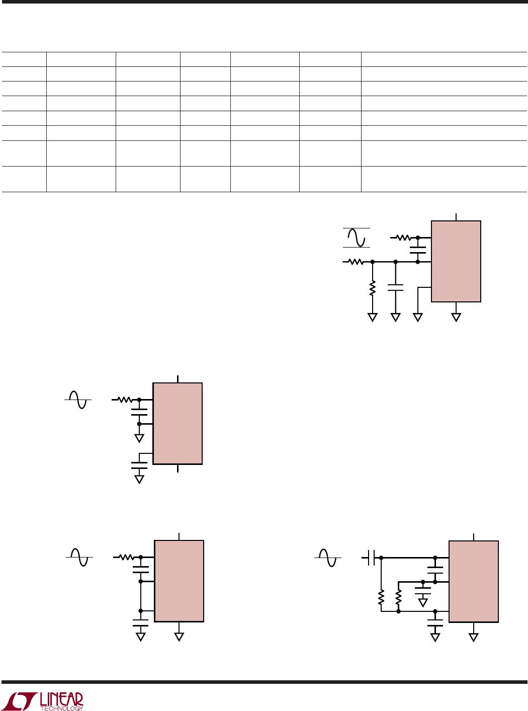
Input Filtering
The noise and the distortion of the input amplifier and
other circuitry must be considered since they will add to
the LTC1405 noise and distortion. The small-signal band-
width of the sample-and-hold circuit is 100MHz. Any noise
or distortion products that are present at the analog inputs
will be summed over this entire bandwidth. Noisy input
circuitry should be filtered prior to the analog inputs to
minimize noise. A simple 1-pole RC filter is sufficient for
many applications.
For example, Figure 9 shows a 1000pF capacitor from
+A
IN
to –A
IN
and a 30Ω source resistor to limit the input
bandwidth to 5.3MHz. The 1000pF capacitor also acts as
a charge reservoir for the input sample-and-hold and
isolates the amplifier driving V
IN
from the ADC’s small
current glitch. In undersampling applications, an input
capacitor this large may prohibitively limit the input band-
width. If this is the case, use as large an input capacitance
as possible. High quality capacitors and resistors should
be used since these components can add distortion. NPO
and silver mica type dielectric capacitors have excellent
linearity. Carbon surface mount resistors can generate
distortion from self-heating and from damage that may
occur during soldering. Metal film surface mount resis-
tors are much less susceptible to both problems.
APPLICATIO S I FOR ATIO
WUU
U
1405 F08a
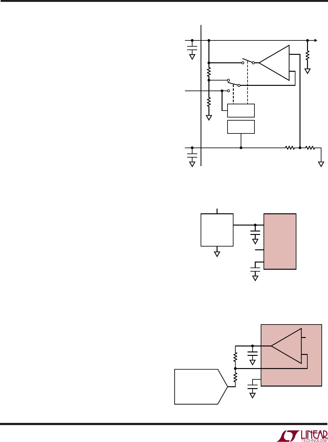
+A
IN
V
SS
V
IN
1000pF
15Ω
15Ω
MINI CIRCUITS
T1-1T
1µF
LTC1405
5V
–A
IN
V
CM
1405 F08b
+A
IN
V
SS
V
IN
MINI CIRCUITS
T1-1T
1µF
LTC1405
5V
–5V
–A
IN
V
CM
1000pF
15Ω
15Ω
Figure 8a. Single Supply Transformer Coupled Input
Figure 8b. Dual Supply Transformer Coupled Input
+A
IN
V
IN
LTC1405
1405 F09
–A
IN
1000pF
30Ω
Choosing an Input Amplifier
Choosing an input amplifier is easy if a few requirements
are taken into consideration. First, to limit the magnitude
of the voltage spike seen by the amplifier from charging
the sampling capacitor, choose an amplifier that has a low
output impedance (<100Ω) at the closed-loop bandwidth
frequency. For example, if an amplifier is used in a gain of
1 and has a unity-gain bandwidth of 50MHz, then the
output impedance at 50MHz must be less than 100Ω. The
second requirement is that the closed-loop bandwidth
Figure 9. RC Input Filter