4
LTC1405
1405fa
DIGITAL I PUTS AND OUTPUTS
UU
The denotes the specifications which apply over the full operating
temperature range, otherwise specifications are at T
A
= 25°C. Specifications are guaranteed for both dual supply and single supply
operation. (Note 5)
SYMBOL PARAMETER CONDITIONS MIN TYP MAX UNITS
POWER REQUIRE E TS
W
U
The denotes the specifications which apply over the full operating temperature
range, otherwise specifications are at T
A
= 25°C. Specifications are guaranteed for both dual supply and single supply operation.
(Note 5)
SYMBOL PARAMETER CONDITIONS MIN TYP MAX UNITS
V
DD
Positive Supply Voltage (Note 10) 4.75 5.25 V
V
SS
Negative Supply Voltage Dual Supply Mode 5.25 4.75 V
Single Supply Mode 0 V
I
DD
Positive Supply Current 23 28 mA
I
SS
Negative Supply Current 0.8 1.2 mA
P
D
Power Dissipation 115 145 mW
TI I G CHARACTERISTICS
W
U
The denotes the specifications which apply over the full operating temperature
range, otherwise specifications are at T
A
= 25°C. Specifications are guaranteed for both dual supply and single supply operation.
(Note 5)
SYMBOL PARAMETER CONDITIONS MIN TYP MAX UNITS
f
SAMPLE
Sampling Frequency 0.02 5 MHz
t
CONV
Conversion Time 150 180 ns
t
ACQ
Acquisition Time 20 50 ns
t
H
CLK High Time (Note 9) 20 100 ns
t
L
CLK Low Time (Note 9) 20 100 ns
t
AD
Aperture Delay of Sample-and-Hold 250 ps
Note 1: Absolute Maximum Ratings are those values beyond which the life
of a device may be impaired.
Note 2: All voltage values are with respect to ground with GND and OGND
wired together (unless otherwise noted).
Note 3: When these pin voltages are taken below V
SS
or above V
DD
, they
will be clamped by internal diodes. This product can handle input currents
greater than 100mA below V
SS
or above V
DD
without latchup.
Note 4: When these pin voltages are taken below V
SS
they will be clamped
by internal diodes. This product can handle input currents greater than
100mA below V
SS
without latchup. GAIN is not clamped to V
DD
. When CLK
is taken above V
DD
, it will be clamped by an internal diode. The CLK pin
can handle input currents of greater than 100mA above V
DD
without
latchup.
Note 5: V
DD
= 5V, V
SS
= –5V or 0V, f
SAMPLE
= 5MHz, t
r
= t
f
= 5ns unless
otherwise specified.
I
IN
Digital Input Current V
IN
= 0V to V
DD
±10 µA
C
IN
Digital Input Capacitance 1.8 pF
V
OH
High Level Output Voltage 0V
DD
= 4.75V, I
O
= –10µA 4.74 V
0V
DD
= 4.75V, I
O
= –200µA 4.0 4.71 V
0V
DD
= 2.7V, I
O
= –10µA 2.6 V
0V
DD
= 2.7V, I
O
= –200µA 2.3 V
V
OL
Low Level Output Voltage 0V
DD
= 4.75V, I
O
= 160µA 0.05 V
0V
DD
= 4.75V, I
O
= 1.6mA 0.10 0.4 V
0V
DD
= 2.7V, I
O
= 160µA 0.05 V
0V
DD
= 2.7V, I
O
= 1.6mA 0.10 0.4 V
I
SOURCE
Output Source Current V
OUT
= 0V 50 mA
I
SINK
Output Sink Current V
OUT
= V
DD
35 mA
5
LTC1405
1405fa
Note 6: Dynamic specifications are guaranteed for dual supply operation
with a single-ended +A
IN
input and –A
IN
grounded. For single supply
dynamic specifications, refer to the Typical Performance Characteristics.
Note 7: Integral nonlinearity is defined as the deviation of a code from a
straight line passing through the actual endpoints of the transfer curve.
The deviation is measured from the center of the quantization band.
Note 8: Bipolar offset is the offset voltage measured from –0.5LSB
when the output code flickers between 0000 0000 0000 and
1111 1111 1111.
Note 9: Guaranteed by design, not subject to test.
Note 10: Recommended operating conditions.
ELECTRICAL CHARACTERISTICS
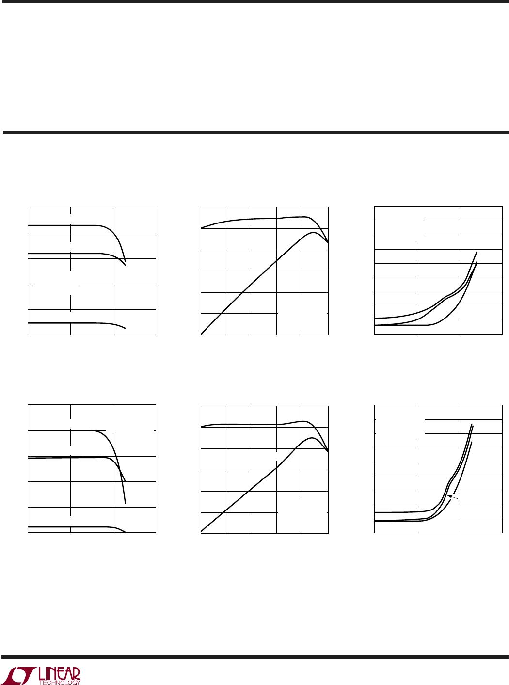
TYPICAL PERFORMANCE CHARACTERISTICS
UW
INPUT FREQUENCY (MHz)
0.1
S/(N + D) (dB)
60
65
1405 G01
55
50
1
10
100
75
70
V
IN
= 0dB
V
IN
= –6dB
V
IN
= –20dB
DUAL SUPPLIES
±2.048V RANGE
GAIN = 1×
INPUT FREQUENCY (MHz)
0.1
S/(N + D) (dB)
60
65
1405 G04
55
50
1
10
100
75
70
V
IN
= 0dB
V
IN
= –6dB
V
IN
= –20dB
SINGLE SUPPLY
±1.024V RANGE
GAIN = 2×
INPUT AMPLITUDE (dBFS)
–50
40
SFDR (dBc AND dBFS)
50
60
70
80
90
100
dBFS
dBc
–40 –30 –20 –10
1405 G02
0
DUAL SUPPLIES
±2.048V RANGE
GAIN = 1×
f
IN
= 2.5MHz
INPUT FREQUENCY (MHz)
0
–95
DISTORTION (dB)
–90
–80
–75
–70
10
–50
1405 G03
–85
1 100
–65
–60
–55
THD
3RD
2ND
DUAL SUPPLIES
±2.048V RANGE
GAIN = 1×
A
IN
= 0dBFS
INPUT AMPLITUDE (dBFS)
–50
40
SFDR (dBc AND dBFS)
50
60
70
80
90
100
dBFS
–40 –30 –20 –10
1405 G05
0
SINGLE SUPPLY
±1.024V RANGE
GAIN = 2×
f
IN
= 2.5MHz
dBc
INPUT FREQUENCY (MHz)
0
–95
DISTORTION (dB)
–90
–80
–75
–70
10
–50
1405 G06
–85
1 100
–65
–60
–55
THD
2ND
3RD
SINGLE SUPPLY
±1.024V RANGE
GAIN = 2×
A
IN
= 0dBFS
S/(N+D) vs Input Frequency
and Amplitude
S/(N+D) vs Input Frequency
and Amplitude
Spurious-Free Dynamic Range
vs Input Amplitude
Distortion vs Input Frequency
Spurious-Free Dynamic Range
vs Input Amplitude
Distortion vs Input Frequency
6
LTC1405
1405fa
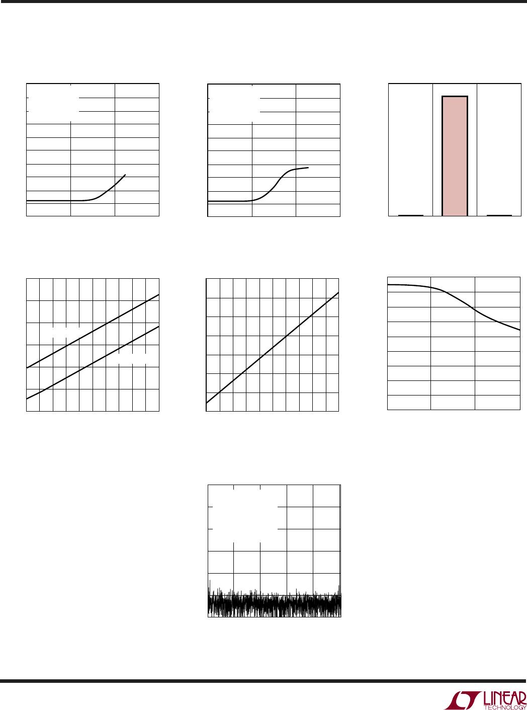
TYPICAL PERFORMANCE CHARACTERISTICS
UW
INPUT FREQUENCY (MHz)
0.1
100
SFDR (dB)
–90
–85
–80
–75
–70
–65
1
10
1405 F07
–60
–55
–50
–95
100
DUAL SUPPLIES
±2.048V RANGE
GAIN = 1×
A
IN
= 0dBFS
INPUT FREQUENCY (MHz)
0.1
100
SFDR (dB)
–90
–85
–80
–75
–70
–65
1
10
1405 F08
–60
–55
–50
–95
100
SINGLE SUPPLY
±1.024V RANGE
GAIN = 2×
A
IN
= 0dBFS
CODE
N – 1
1570
410554
V
REF
= 4.096V
GAIN = 1×
HITS
N
N + 1
1420 F09
1572
CLOCK FREQUENCY (MHz)
0 0.5 1.5 2.5 3.5 4.5
I
DD
(mA)
23
22
21
20
19
18
17
1.0 2.0 3.0 4.0
1405 G10
5.0
V
REF
= 4.096V
V
REF
= 2.048V
I
SS
(mA)
0.7
0.6
0.5
0.4
0.3
0.2
0.1
0
CLOCK FREQUENCY (MHz)
0 0.5 1.5 2.5 3.5 4.51.0 2.0 3.0 4.0
1405 G11
5.0
INPUT FREQUENCY (MHz)
0.01
0
CMRR (dB)
10
30
40
50
1
90
1405 G12
20
0.1 10
60
70
80
FREQUENCY (MHz)
0
AMPLITUDE (dB)
0
–20
–40
–60
–80
–100
–120
0.5 1.0 1.5 2.0
1405 • G13
2.5
I
DD
vs Clock Frequency I
SS
vs Clock Frequency
CMRR vs Input Frequency
LTC1405 Nonaveraged 4096
Point FFT
SFDR vs Input Frequency,
Differential Input Grounded Input Histogram
SFDR vs Input Frequency,
Differential Input
f
SAMPLE
= 5Msps
f
IN
= 2.515869141MHz
SFDR = 86.2dB
SINAD = 71.3dB
V
IN
= 4V
P-P
± 5V SUPPLIES

LTC1405CGN#TRPBF

Mfr. #:
Manufacturer:
Analog Devices Inc.
Description:
Analog to Digital Converters - ADC 12-B, 5Msps, Smpl ADC
Lifecycle:
New from this manufacturer.
Delivery:
DHL FedEx Ups TNT EMS
Payment:
T/T Paypal Visa MoneyGram Western Union

Products related to this Datasheet