13
LTC1405
1405fa
Digital Outputs and Overflow Bit (OF)
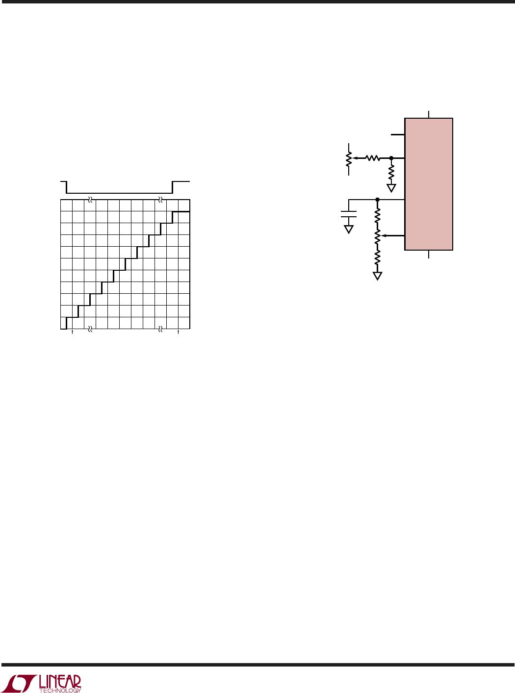
Figure 10 shows the ideal input/output characteristics for
the LTC1405. The output data is two’s complement binary
for all input ranges and for both single and dual supply
operation. One LSB = V
REF
/4.096. To create a straight
binary output, invert the MSB (D11). The overflow bit (OF)
indicates when the analog input is outside the input range
of the converter. OF is high when the output code is 1000
0000 0000 or 0111 1111 1111.
APPLICATIO S I FOR ATIO
WUU
U
noise from affecting performance, the load capacitance on
the digital outputs should be minimized. If large capacitive
loads are required, (>30pF) external buffers or 100Ω
resistors in series with the digital outputs are suggested.
INPUT VOLTAGE (V)
–(FS – 1LSB) FS – 1LSB
OUTPUT CODE
1405 F10
011…111
011…110
011…101
100…010
100…001
100…000
OVERFLOW
BIT
1
0
Figure 10. LTC1405 Transfer Characteristics
R2
1k
10k1µF
1405 F11
+A
IN
V
SS
V
IN
5V
–5V
–5V
LTC1405
5V
–A
IN
SENSE
V
REF
10k
24k
100Ω
R1
50k
Full-Scale and Offset Adjustment
In applications where absolute accuracy is important,
offset and full-scale errors can be adjusted to zero. Offset
error should be adjusted before full-scale error. Figure 11
shows a method for error adjustment for a dual supply,
4.096V application. For zero offset error apply –0.5mV
(i. e., – 0.5LSB) at +A
IN
and adjust R1 until the output code
flickers between 0000 0000 0000 and 1111 1111 1111.
For full-scale adjustment, apply an input voltage of 2.0465V
(FS – 1.5LSBs) at +A
IN
and adjust R2 until the output code
flickers between 0111 1111 1110 and 0111 1111 1111.
Digital Output Drivers
The LTC1405 output drivers can interface to logic operat-
ing from 3V to 5V by setting OV
DD
to the logic power
supply. If 5V output is desired, OV
DD
can be shorted to V
DD
and share its decoupling capacitor. Otherwise, OV
DD
re-
quires its own 1µF decoupling capacitor. To prevent digital
Timing
The conversion start is controlled by the rising edge of the
CLK pin. Once a conversion is started it cannot be stopped
or restarted until the conversion cycle is complete. Output
data is updated at the end of conversion, or about 150ns
after a conversion is begun. There is an additional two
cycle pipeline delay, so the data for a given conversion is
output two full clock cycles plus 150ns after the convert
start. Thus output data can be latched on the third CLK
rising edge after the rising edge that samples the input.
Clock Input
The LTC1405 only uses the rising edge of the CLK pin for
internal timing, and CLK doesn’t necessarily need to have
a 50% duty cycle. For optimal AC performance the rise
time of the CLK should be less than 5ns. If the available
clock has a rise time slower than 5ns, it can be locally sped
up with a logic gate. With single supply operation the clock
can be driven with 5V CMOS, 3V CMOS or TTL logic levels.
With dual power supplies the clock should be driven with
5V CMOS levels.
As with all fast ADCs, the noise performance of the
LTC1405 is sensitive to clock jitter when high speed inputs
Figure 11. Offset and Full-Scale Adjust Circuit