DS1080LU+

General Description
The DS1080L is a low-jitter, crystal-based clock gener-
ator with an integrated phase-locked loop (PLL) to gen-
erate spread-spectrum clock outputs from 16MHz to
134MHz. The device is pin-programmable to select the
clock multiplier rate as well as the dither magnitude.
The DS1080L has a spread-spectrum disable mode
and a power-down mode to conserve power.
Applications
Automotive
Cable Modems
Cell Phones
Computer Peripherals
Copiers
Infotainment
PCs
Printers
Features
! Generates Spread-Spectrum Clocks from 16MHz
to 134MHz
! Selectable Clock Multiplier Rates of 1x, 2x, and 4x
! Center Spread-Spectrum Dithering
! Selectable Spread-Spectrum Modulation
Magnitudes of ±0.5%, ±1.0%, and ±1.5%
! Spread-Spectrum Disable Mode
! Low Cycle-to-Cycle Jitter
! Power-Down Mode with High-Impedance Output
! Low Power Consumption
! 3.0V to 3.6V Single-Supply Operation
! -40°C to +125°C Temperature Operation
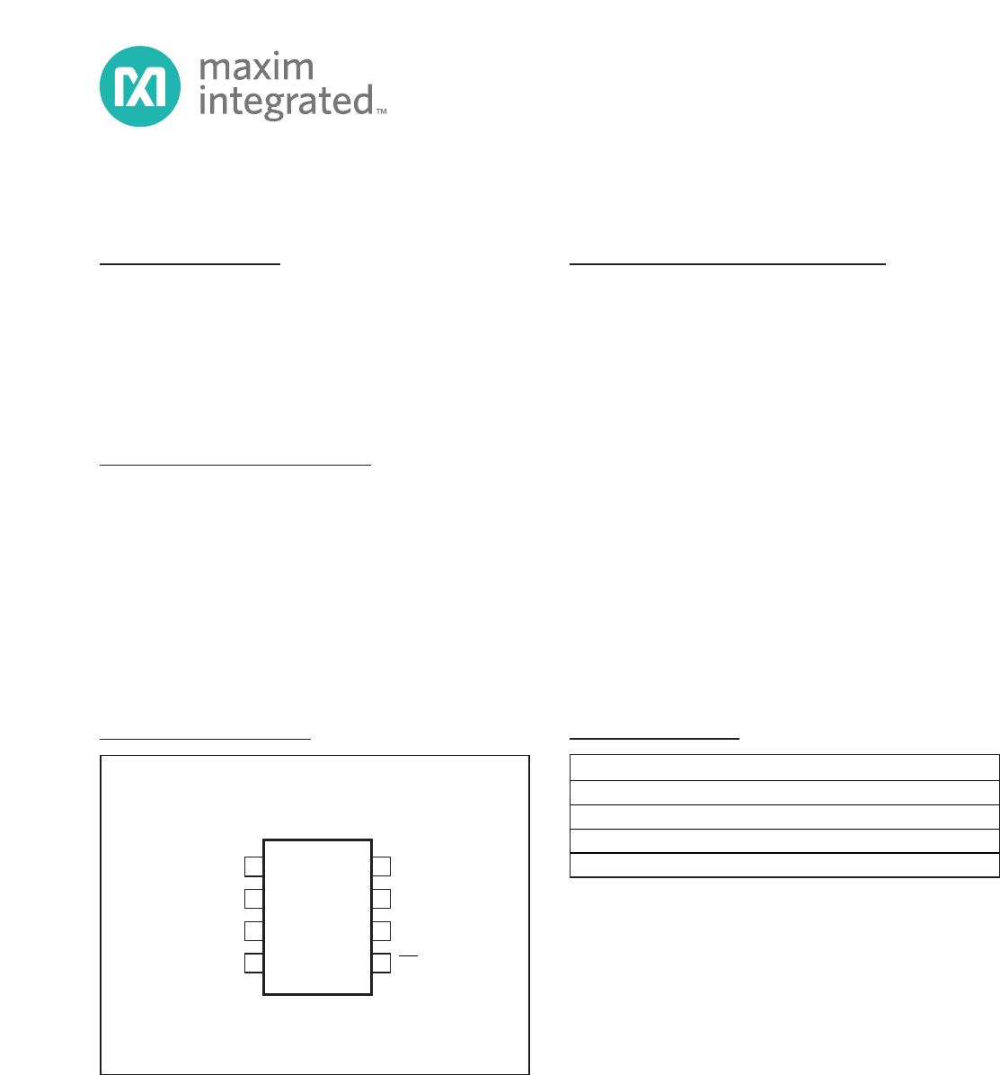
! Small 8-Lead µSOP Package
Spread-Spectrum Crystal Multiplier
DS1080L
For pricing, delivery, and ordering information, please contact Maxim Direct at
1-888-629-4642, or visit Maxim Integrated’s website at www.maximintegrated.com.
SSO
PDNSMSEL
1
+
2
8
7
X2
V
CC
GND
CMSEL
X1
µSOP
TOP VIEW
3
4
6
5
DS1080L
Pin Configuration
19-4997; Rev 5; 3/13
+
Denotes a lead(Pb)-free/RoHS-compliant package.
/V denotes an automotive qualified part.
T = Tape and reel.
Ordering Information
PART TEMP RANGE PIN-PACKAGE
DS1080LU+ -40°C to +125°C 8 µSOP
DS1080LU/V+ -40°C to +125°C 8 µSOP
DS1080LU/V+T -40°C to +125°C 8 µSOP
DS1080LU+T -40°C to +125°C 8 µSOP
Spread-Spectrum Crystal Multiplier
2 Maxim Integrated
DS1080L
ABSOLUTE MAXIMUM RATINGS
RECOMMENDED OPERATING CONDITIONS
(T
A
= -40°C to +125°C, unless otherwise noted.)
Stresses beyond those listed under “Absolute Maximum Ratings” may cause permanent damage to the device. These are stress ratings only, and functional
operation of the device at these or any other conditions beyond those indicated in the operational sections of the specifications is not implied. Exposure to
absolute maximum rating conditions for extended periods may affect device reliability.
Voltage on V
CC
Relative to GND...........................-0.3V to +4.3V
Voltage on Any Lead Relative
to GND .................-0.3V to (V
CC
+ 0.3V), not to exceed +4.3V
Continuous Power Dissipation (T
A
= +70°C)
µSOP (derate 4.5mW/°C above +70°C).......................362mW
Operating Temperature Range .........................-40°C to +125°C
Storage Temperature Range .............................-55°C to +125°C
Lead Temperature (soldering, 10s) .................................+300°C
Soldering Temperature (reflow) .......................................+260°C
PARAMETER SYMBOL CONDITIONS MIN TYP MAX UNITS
Supply Voltage V
CC
(Note 1) 3.0 3.6 V
Input Logic 1 V
IH
0.8 x
V
CC
V
CC
+
0.3
V
Input Logic 0 V
IL
V
GND
-
0.3
0.2 x
V
CC
V
Input Logic Open I
IF
0V < V
IN
< V
CC
(Note 2) ±1 µA
Input Leakage I
IL
0V < V
IN
< V
CC
(Note 3) ±80 µA
f
SSO
< 67MHz 15
67MHz f
SSO
< 101MHz 10
SSO Load C
SSO
101MHz f
SSO
< 134MHz 7
pF
Crystal or Clock Input
Frequency
f
IN
16.0 33.4 MHz
Crystal ESR X
ESR
90
Clock Input Duty Cycle F
INDC
40 60 %
Crystal Parallel Load
Capacitance
C
L
(Note 4) 18 pF
DC ELECTRICAL CHARACTERISTICS
(V
CC
= +3.0V to +3.6V, T
A
= -40°C to +125°C, unless otherwise noted.)
PARAMETER SYMBOL CONDITIONS MIN TYP MAX UNITS
Supply Curr ent I
CC1
C
SSO
= 15pF, SSO = 16MHz 15 mA
Power-Down Current I
CCQ
PDN = GND, all input pins open 200 µA
Output Leakage (SSO) I
OZ
PDN = GND -1 +1 µA
Low-Level Outp ut Voltage
(SS O)
V
OL
I
OL
= 4mA 0.4 V
High-Level Output Voltage
(SS O)
V
OH
I
OH
= -4mA 2.4 V
Input Capacitance (X1/X2) C
IN
(Note 5) 5 pF
Spread-Spectrum Crystal Multiplier
Maxim Integrated 3
DS1080L
AC ELECTRICAL CHARACTERISTICS
(V
CC
= +3.0 to +3.6V, T
A
= -40°C to +125°C, unless otherwise noted.)
PARAMETER SYMBOL CONDITIONS MIN TYP MAX UNITS
Measured at V
CC
/2, CMSEL = 0 or ope n 40 60
SSO Duty Cycle SSODC
Measured at V
CC
/2, CMSEL = 1 30 70
%
Rise Time t
R
(Note 6) 1.6 ns
Fall Time t
F
(Note 6) 1.6 ns
Peak Cycle-to-Cycle Jitter t
J
f
SSO
= 16MHz, T
A
= -40 to +85°C,
10,000 cycles ( Note 5)
75 ps
16MHz 20
Power-Up Time t
POR
PDN pin (Note 7)
33.4MHz 11
ms
Power-Down Time t
PDN
PDN pin (Notes 8 and 9) 100 ns
Dither R ate f
DITHER
(Note 9) f
IN
/992
Note 1: All voltages referenced to ground.
Note 2: Maximum source/sink current applied to input to be considered an open. Typical voltage range between 0.4 x V
CC
and 0.55
x V
CC
.
Note 3: Applicable to pins CMSEL, SMSEL, and PDN.
Note 4: See information about C
L1
and C
L2
in the
Applications Information
section at the end of the data sheet.
Note 5: Not production tested.
Note 6: For 7pF load.
Note 7: Time between PDN deasserted to output active.
Note 8: Time between PDN asserted to output high impedance.
Note 9: Guaranteed by design.

DS1080LU+

Mfr. #:
Manufacturer:
Maxim Integrated
Description:
Clock Generators & Support Products Spread-Spectrum Crystal Multiplier
Lifecycle:
New from this manufacturer.
Delivery:
DHL FedEx Ups TNT EMS
Payment:
T/T Paypal Visa MoneyGram Western Union

Products related to this Datasheet