© Semiconductor Components Industries, LLC, 2010
October, 2010 − Rev. 13
1 Publication Order Number:
NBC12430/D
NBC12430, NBC12430A
3.3V/5V Programmable PLL
Synthesized Clock
Generator
50 MHz to 800 MHz
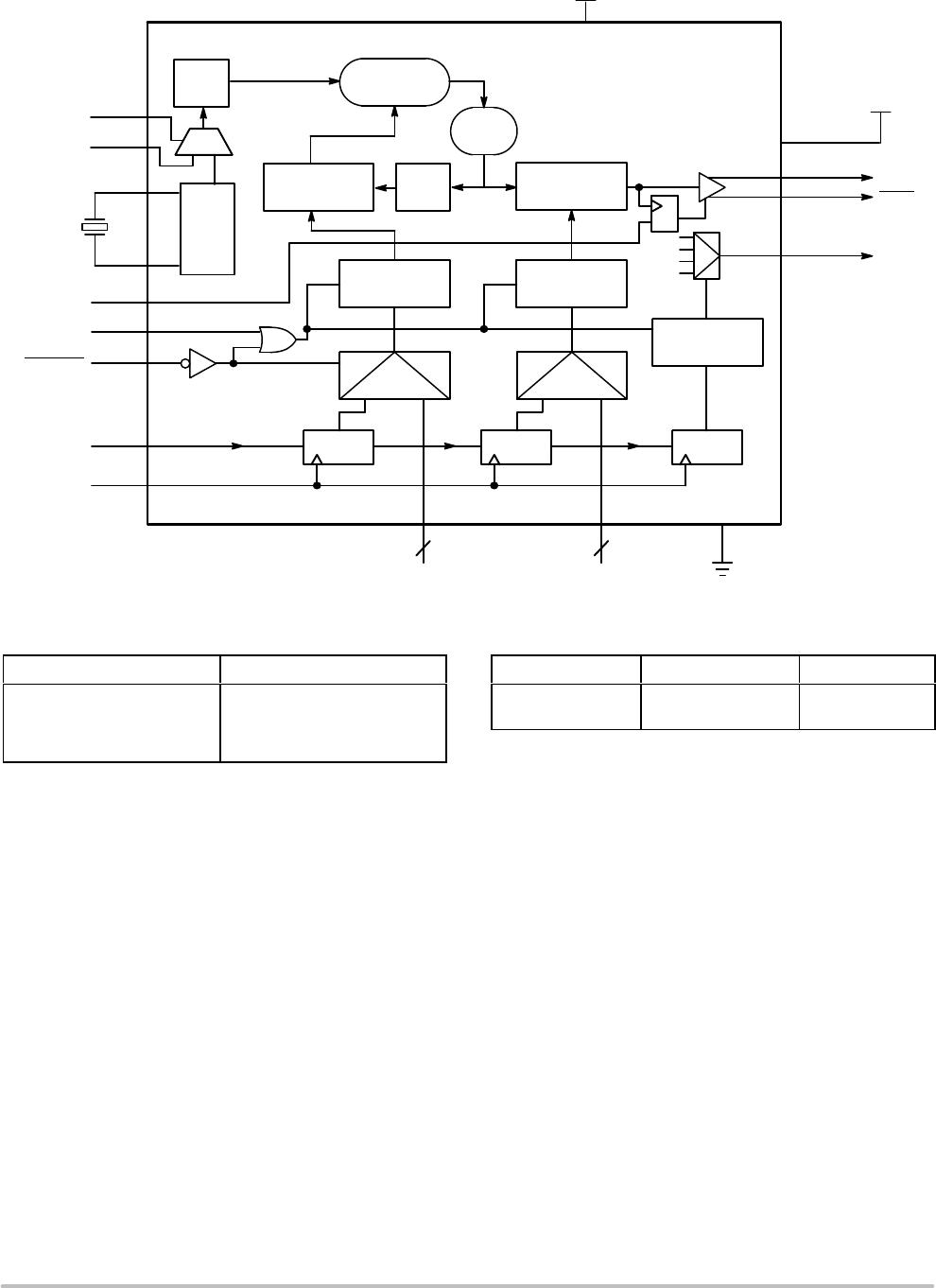
The NBC12430 and NBC12430A are general purpose, PLL based
synthesized clock sources. The VCO will operate over a frequency
range of 400 MHz to 800 MHz. The VCO frequency is sent to the
N−output divider, where it can be configured to provide division ratios
of 1, 2, 4, or 8. The VCO and output frequency can be programmed
using the parallel or serial interfaces to the configuration logic. Output
frequency steps of 250 kHz, 500 kHz, 1.0 MHz, 2.0 MHz can be
achieved using a 16 MHz crystal, depending on the output dividers
settings. The PLL loop filter is fully integrated and does not require
any external components.
Features
• Best−in−Class Output Jitter Performance, ±20 ps Peak−to−Peak
• 50 MHz to 800 MHz Programmable Differential PECL Outputs
• Fully Integrated Phase−Lock−Loop with Internal Loop Filter
• Parallel Interface for Programming Counter and Output Dividers
During Powerup
• Minimal Frequency Overshoot
• Serial 3−Wire Programming Interface
• Crystal Oscillator Interface
• Operating Range: V
CC
= 3.135 V to 5.25 V
• CMOS and TTL Compatible Control Inputs
• Pin and Function Compatible with Motorola MC12430 and
MPC9230
• 0°C to 70°C Ambient Operating Temperature (NBC12430)
• −40°C to 85°C Ambient Operating Temperature (NBC12430A)
• Pb−Free Packages are Available
MARKING
DIAGRAMS
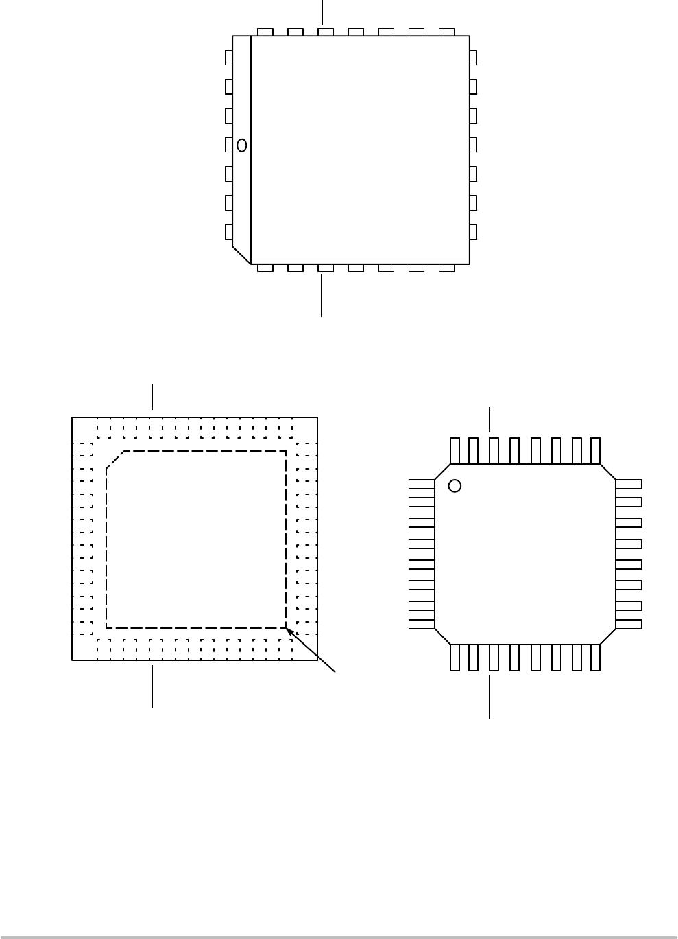
PLCC−28
FN SUFFIX
CASE 776
NBC12430xG
AWLYYWW
128
http://onsemi.com
See detailed ordering and shipping information in the package
dimensions section on page 16 of this data sheet.
ORDERING INFORMATION
LQFP−32
FA SUFFIX
CASE 873A
x = Blank or A
A = Assembly Location
WL, L = Wafer Lot
YY, Y = Year
WW, W = Work Week
G or G = Pb−Free Package
NBC12
430x
AWLYYWWG
QFN32
MN SUFFIX
CASE 488AM
32
1
NBC12
430x
AWLYYWWG
G
1
(Note: Microdot may be in either location)