NBC12430, NBC12430A
http://onsemi.com
7
Table 8. AC CHARACTERISTICS (V
CC
= 3.135 V to 5.25 V ± 5%; T
A
= 0°C to 70°C (NBC12430), T
A
= 40°C to 85°C (NBC12430A))
(Note 7)
Symbol
Characteristic Condition Min Max Unit
F
MAXI
Maximum Input Frequency S_CLOCK
XTAL Oscillator
FREF_EXT (Note 8)
(Note 6)
10
10
10
20
100
MHz
F
MAXO
Maximum Output Frequency VCO (Internal)
F
OUT
400
50
800
800
MHz
t
LOCK
Maximum PLL Lock Time 10 ms
t
jitter(pd)
Period Jitter (RMS) (1s)
50 MHz f
OUT
< 100 MHz
100 MHz f
OUT
< 800 MHz
8
5
ps
t
jitter(cyccyc)
CycletoCycle Jitter (PeaktoPeak) (8s)
50 MHz f
OUT
< 100 MHz
100 MHz f
OUT
< 800 MHz
40
20
ps
t
s
Setup Time S_DATA to S_CLOCK
S_CLOCK to S_LOAD
M, N to P_LOAD
20
20
20
ns
t
h
Hold Time S_DATA to S_CLOCK
M, N to P_LOAD
20
20
ns
tpw
MIN
Minimum Pulse Width S_LOAD
P_LOAD
50
50
ns
DCO Output Duty Cycle 47.5 52.5 %
t
r
, t
f
Output Rise/Fall F
OUT
20%80% 175 425 ps
NOTE: Device will meet the specifications after thermal equilibrium has been established when mounted in a test socket or printed circuit
board with maintained transverse airflow greater than 500 lfpm. Electrical parameters are guaranteed only over the declared
operating temperature range. Functional operation of the device exceeding these conditions is not implied. Device specification limit
values are applied individually under normal operating conditions and not valid simultaneously.
6. 10 MHz is the maximum frequency to load the feedback divide registers. S_CLOCK can be switched at higher frequencies when used as
a test clock in TEST_MODE 6.
7. F
OUT/
F
OUT
and TEST outputs are terminated through a 50 W resistor to V
CC
2.0 V.
8. Maximum frequency on FREF_EXT is a function of setting the appropriate M counter value for the VCO to operate within the valid range
of 400 MHz f
VCO
800 MHz. (See Table 11)
NBC12430, NBC12430A
http://onsemi.com
8
FUNCTIONAL DESCRIPTION
The internal oscillator uses the external quartz crystal as
the basis of its frequency reference. The output of the
reference oscillator is divided by 16 before being sent to the
phase detector. With a 16 MHz crystal, this provides a
reference frequency of 1 MHz. Although this data sheet
illustrates functionality only for a 16 MHz crystal, Table 9,
any crystal in the 1020 MHz range can be used, Table 11.
The VCO within the PLL operates over a range of 400 to
800 MHz. Its output is scaled by a divider that is configured
by either the serial or parallel interfaces. The output of this
loop divider is also applied to the phase detector.
The phase detector and the loop filter force the VCO
output frequency to be M times the reference frequency by
adjusting the VCO control voltage. Note that for some
values of M (either too high or too low), the PLL will not
achieve loop lock.
The output of the VCO is also passed through an output
divider before being sent to the PECL output driver. This
output divider (N divider) is configured through either the
serial or the parallel interfaces and can provide one of four
division ratios (1, 2, 4, or 8). This divider extends the
performance of the part while providing a 50% duty cycle.
The output driver is driven differentially from the output
divider and is capable of driving a pair of transmission lines
terminated into 50 W to V
CC
2.0 V. The positive reference
for the output driver and the internal logic is separated from
the power supply for the phaselocked loop to minimize
noise induced jitter.
The configuration logic has two sections: serial and
parallel. The parallel interface uses the values at the M[8:0]
and N[1:0] inputs to configure the internal counters.
Normally upon system reset, the P_LOAD
input is held
LOW until sometime after power becomes valid. On the
LOWtoHIGH transition of P_LOAD
, the parallel inputs
are captured. The parallel interface has priority over the
serial interface. Internal pullup resistors are provided on the
M[8:0] and N[1:0] inputs to reduce component count in the
application of the chip.
The serial interface logic is implemented with a fourteen
bit shift register scheme. The register shifts once per rising
edge of the S_CLOCK input. The serial input S_DATA must
meet setup and hold timing as specified in the AC
Characteristics section of this document. With P_LOAD
held high, the configuration latches will capture the value of
the shift register on the HIGHtoLOW edge of the
S_LOAD input. See the programming section for more
information.
The TEST output reflects various internal node values and
is controlled by the T[2:0] bits in the serial data stream. See
the programming section for more information.
Table 9. Programming VCO Frequency Function Table with 16 MHz Crystal.
VCO
Frequency
(MHz)
M
Count
Divisor
256 128 64 32 16 8 4 2 1
M8 M7 M6 M5 M4 M3 M2 M1 M0
400 200 0 1 1 0 0 1 0 0 0
402 201 0 1 1 0 0 1 0 0 1
404 202 0 1 1 0 0 1 0 1 0
406 203 0 1 1 0 0 1 0 1 1
794 397 1 1 0 0 0 1 1 0 1
796 398 1 1 0 0 0 1 1 1 0
798 399 1 1 0 0 0 1 1 1 1
800 400 1 1 0 0 1 0 0 0 0
NBC12430, NBC12430A
http://onsemi.com
9
PROGRAMMING INTERFACE
Programming the NBC12430 and NBC12430A is
accomplished by properly configuring the internal dividers
to produce the desired frequency at the outputs. The output
frequency can by represented by this formula:
F
OUT
((F
XTAL
or F
REF_EXT
) 16) 2M N
(eq. 1)
where F
XTAL
is the crystal frequency, M is the loop divider
modulus, and N is the output divider modulus. Note that it
is possible to select values of M such that the PLL is unable
to achieve loop lock. To avoid this, always make sure that M
is selected to be 200 M 400 for a 16 MHz input reference.
Assuming that a 16 MHz reference frequency is used the
above equation reduces to:
F
OUT
2M N
(eq. 2)
Substituting the four values for N (1, 2, 4, 8) yields:
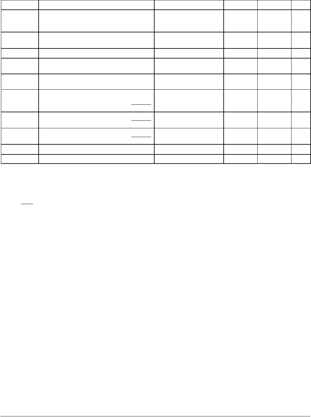
Table 10. Programmable Output Divider Function
Table
N1 N0
N
Divider
F
OUT
Output
Frequency
Range (MHz)*
F
OUT
Step
1 1 1 M 2 400800 2 MHz
0 0 2 M 200400 1 MHz
0 1 4 M 2 100200 500 kHz
1 0 8 M 4 50100 250 kHz
*For crystal frequency of 16 MHz.
The user can identify the proper M and N values for the
desired frequency from the above equations. The four output
frequency ranges established by N are 400800 MHz,
200400 MHz, 100200 MHz and 50100 MHz, respectively.
From these ranges, the user will establish the value of N
required. The value of M can then be calculated based on
equation 1. For example, if an output frequency of 131 MHz
was desired, the following steps would be taken to identify the
appropriate M and N values. 131 MHz falls within the
frequency range set by an N value of 4; thus, N [1:0] = 01.
For N = 4, F
OUT
= M ÷ 2 and M = 2 x F
OUT
. Therefore,
M = 131 x 2 = 262, so M[8:0] = 100000110. Following this
same procedure, a user can generate any whole frequency
desired between 50 and 800 MHz. Note that for N > 2,
fractional values of F
OUT
can be realized. The size of the
programmable frequency steps (and thus, the indicator of the
fractional output frequencies achievable) will be equal to
F
XTAL
÷ 16 ÷ N.
For input reference frequencies other than 16 MHz, see
Table 11, which shows the usable VCO frequency and M
divider range.
The input frequency and the selection of the feedback
divider M is limited by the VCO frequency range and
F
XTAL
. M must be configured to match the VCO frequency
range of 400 to 800 MHz in order to achieve stable PLL
operation.
M
min
f
VCOmin
2(f
XTAL
16) and
(eq. 3)
M
max
f
VCOmax
2(f
XTAL
16)
(eq. 4)
The value for M falls within the constraints set for PLL
stability. If the value for M fell outside of the valid range, a
different N value would be selected to move M in the
appropriate direction.
The M and N counters can be loaded either through a
parallel or serial interface. The parallel interface is
controlled via the P_LOAD
signal such that a LOW to HIGH
transition will latch the information present on the M[8:0]
and N[1:0] inputs into the M and N counters. When the
P_LOAD
signal is LOW, the input latches will be
transparent and any changes on the M[8:0] and N[1:0] inputs
will affect the F
OUT
output pair. To use the serial port, the
S_CLOCK signal samples the information on the S_DATA
line and loads it into a 14 bit shift register. Note that the
P_LOAD
signal must be HIGH for the serial load operation
to function. The Test register is loaded with the first three
bits, the N register with the next two, and the M register with
the final nine bits of the data stream on the S_DATA input.
For each register, the most significant bit is loaded first (T2,
N1, and M8). A pulse on the S_LOAD pin after the shift
register is fully loaded will transfer the divide values into the
counters. The HIGH to LOW transition on the S_LOAD
input will latch the new divide values into the counters.
Figures 5 and 6 illustrate the timing diagram for both a
parallel and a serial load of the device synthesizer.
M[8:0] and N[1:0] are normally specified once at
powerup through the parallel interface, and then possibly
again through the serial interface. This approach allows the
application to come up at one frequency and then change or
finetune the clock as the ability to control the serial
interface becomes available.
The TEST output provides visibility for one of the several
internal nodes as determined by the T[2:0] bits in the serial
configuration stream. It is not configurable through the
parallel interface. The T2, T1, and T0 control bits are preset
to ‘000’ when P_LOAD
is LOW so that the PECL F
OUT
outputs are as jitterfree as possible. Any active signal on the
TEST output pin will have detrimental affects on the jitter
of the PECL output pair. In normal operations, jitter
specifications are only guaranteed if the TEST output is
static. The serial configuration port can be used to select one
of the alternate functions for this pin.

NBC12430FAR2G

Mfr. #:
Manufacturer:
ON Semiconductor
Description:
Phase Locked Loops - PLL 3.3V/5V Programmable PLL Clock Generator
Lifecycle:
New from this manufacturer.
Delivery:
DHL FedEx Ups TNT EMS
Payment:
T/T Paypal Visa MoneyGram Western Union