NBC12430, NBC12430A
http://onsemi.com
18
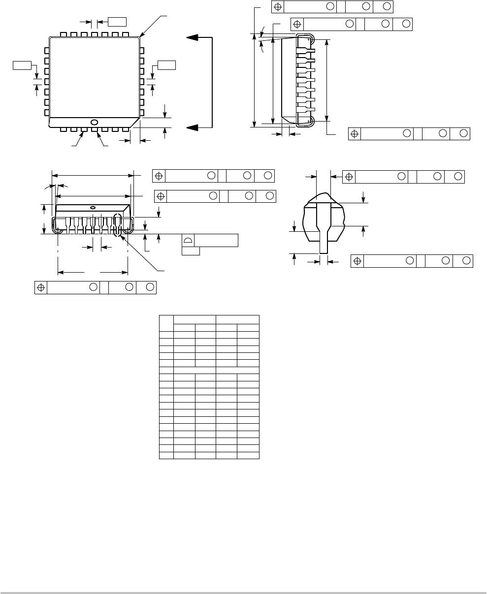
PACKAGE DIMENSIONS
28 LEAD PLLC
CASE 776−02
ISSUE F
−N−
−M−
−L−
V
W
D
D
Y BRK
28 1
VIEW S
S
L-M
S
0.010 (0.250) N
S
T
S
L-M
M
0.007 (0.180) N
S
T
0.004 (0.100)
G1
G
J
C
Z
R
E
A
SEATING
PLANE
S
L-M
M
0.007 (0.180) N
S
T
−T−
B
S
L-M
S
0.010 (0.250) N
S
T
S
L-M
M
0.007 (0.180) N
S
T
U
S
L-M
M
0.007 (0.180) N
S
T
Z
G1X
VIEW D−D
S
L-M
M
0.007 (0.180) N
S
T
K1
VIEW S
H
K
F
S
L-M
M
0.007 (0.180) N
S
T
NOTES:
1. DATUMS -L-, -M-, AND -N- DETERMINED
WHERE TOP OF LEAD SHOULDER EXITS
PLASTIC BODY AT MOLD PARTING LINE.
2. DIMENSION G1, TRUE POSITION TO BE
MEASURED AT DATUM -T-, SEATING PLANE.
3. DIMENSIONS R AND U DO NOT INCLUDE
MOLD FLASH. ALLOWABLE MOLD FLASH IS
0.010 (0.250) PER SIDE.
4. DIMENSIONING AND TOLERANCING PER
ANSI Y14.5M, 1982.
5. CONTROLLING DIMENSION: INCH.
6. THE PACKAGE TOP MAY BE SMALLER THAN
THE PACKAGE BOTTOM BY UP TO 0.012
(0.300). DIMENSIONS R AND U ARE
DETERMINED AT THE OUTERMOST
EXTREMES OF THE PLASTIC BODY
EXCLUSIVE OF MOLD FLASH, TIE BAR
BURRS, GATE BURRS AND INTERLEAD
FLASH, BUT INCLUDING ANY MISMATCH
BETWEEN THE TOP AND BOTTOM OF THE
PLASTIC BODY.
7. DIMENSION H DOES NOT INCLUDE DAMBAR
PROTRUSION OR INTRUSION. THE DAMBAR
PROTRUSION(S) SHALL NOT CAUSE THE H
DIMENSION TO BE GREATER THAN 0.037
(0.940). THE DAMBAR INTRUSION(S) SHALL
NOT CAUSE THE H DIMENSION TO BE
SMALLER THAN 0.025 (0.635).
DIM MIN MAX MIN MAX
MILLIMETERSINCHES
A 0.485 0.495 12.32 12.57
B 0.485 0.495 12.32 12.57
C 0.165 0.180 4.20 4.57
E 0.090 0.110 2.29 2.79
F 0.013 0.021 0.33 0.53
G 0.050 BSC 1.27 BSC
H 0.026 0.032 0.66 0.81
J 0.020 --- 0.51 ---
K 0.025 --- 0.64 ---
R 0.450 0.456 11.43 11.58
U 0.450 0.456 11.43 11.58
V 0.042 0.048 1.07 1.21
W 0.042 0.048 1.07 1.21
X 0.042 0.056 1.07 1.42
Y --- 0.020 --- 0.50
Z 2 10 2 10
G1 0.410 0.430 10.42 10.92
K1 0.040 --- 1.02 ---
__ __