Information furnished by Analog Devices is believed to be accurate and
reliable. However, no responsibility is assumed by Analog Devices for its
use, nor for any infringements of patents or other rights of third parties
that may result from its use. No license is granted by implication or oth-
erwise under any patent or patent rights of Analog Devices. Trademarks
and registered trademarks are the property of their respective owners.
One Technology Way, P.O. Box 9106, Norwood, MA 02062-9106, U.S.A.
Tel: 781/329-4700
www.analog.com
Fax: 781/326-8703 © 2004 Analog Devices, Inc. All rights reserved.
OP275
Dual Bipolar/JFET, Audio
Operational Amplier
FEATURES
Excellent Sonic Characteristics
Low Noise: 6 nV/
Hz
Low Distortion: 0.0006%
High Slew Rate: 22 V/s
Wide Bandwidth: 9 MHz
Low Supply Current: 5 mA
Low Offset Voltage: 1 mV
Low Offset Current: 2 nA
Unity Gain Stable
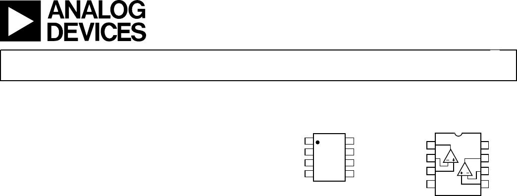
SOIC-8 Package
PDIP-8 Package
APPLICATIONS
High Performance Audio
Active Filters
Fast Ampliers
Integrators
PIN CONNECTIONS
GENERAL DESCRIPTION
The OP275 is the rst amplier to feature the Butler Amplier
front end. This new front end design combines both bipolar
and JFET transistors to attain ampliers with the accuracy and
low noise performance of bipolar transistors, and the speed and
sound quality of JFETs. Total Harmonic Distortion plus Noise
equals that of previous audio ampliers, but at much lower
supply currents.
A very low l/f corner of below 6 Hz maintains a at noise density
response. Whether noise is measured at either 30 Hz or 1 kHz,
it is only 6 nV
Hz. The JFET portion of the input stage gives
the OP275 its high slew rates to keep distortion low, even when
large output swings are required, and the 22 V/µs slew rate of the
OP275 is the fastest of any standard audio amplier. Best of all,
this low noise and high speed are accomplished using less than
5 mA of supply current, lower than any standard audio amplier.
Improved dc performance is also provided with bias and offset
currents greatly reduced over purely bipolar designs. Input offset
voltage is guaranteed at 1 mV and is typically less than 200 µV.
This allows the OP275 to be used in many dc-coupled or sum-
ming applications without the need for special selections or the
added noise of additional offset adjustment circuitry.
The output is capable of driving 600 loads to 10 V rms while
maintaining low distortion. THD + Noise at 3 V rms is a low
0.0006%.
The OP275 is specied over the extended industrial (–40°C to
+85°C) temperature range. OP275s are available in both plas-
tic DIP and SOIC-8 packages. SOIC-8 packages are available
in 2500-piece reels. Many audio ampliers are not offered
in SOIC-8 surface-mount packages for a variety of reasons;
however, the OP275 was designed so that it would offer full
performance in surface-mount packaging.
8-Lead Narrow-Body SOIC
(S Sufx)
OP275
OUT A
–IN A
+IN A
V–
OUT B
–IN B
+IN B
V+
1
2
3
4
5
6
7
8
8-Lead PDIP
(P Sufx)
1
2
3
4
8
7
6
5
OP275
OUT B
–IN B
+IN B
V+OUT A
–IN A
+IN A
V–
REV. C