OP275
–8–
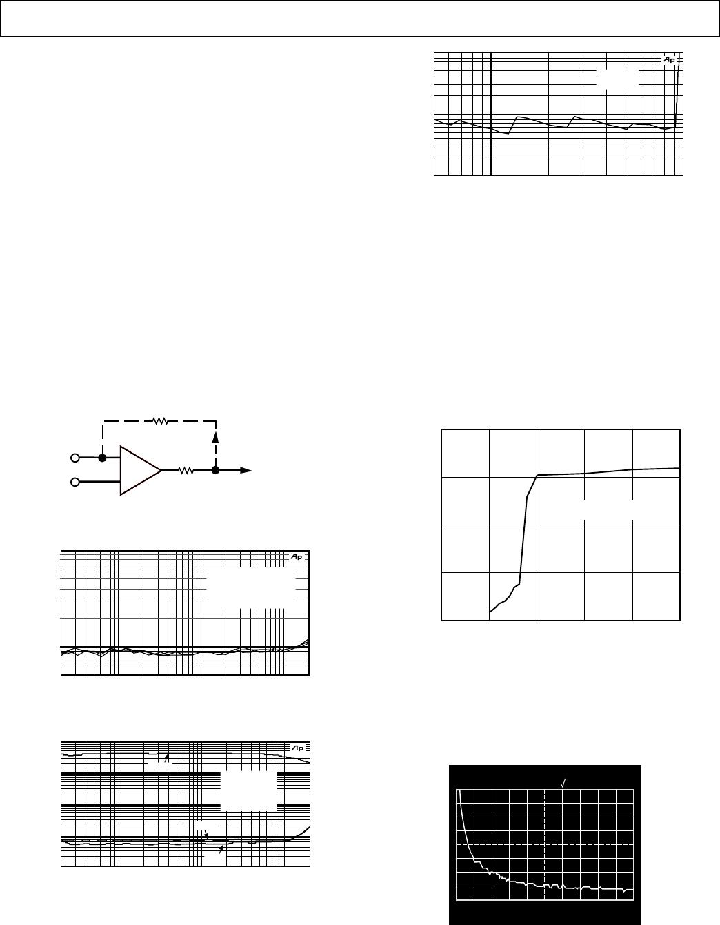
Noise Testing
For audio applications, the noise density is usually the most
important noise parameter. For characterization, the OP275 is
tested using an Audio Precision, System One. The input signal
to the Audio Precision must be amplied enough to measure it
accurately. For the OP275, the noise is gained by approximately
1020 using the circuit shown in Figure 7. Any readings on the
Audio Precision must then be divided by the gain. In imple-
menting this test xture, good supply bypassing is essential.
A
B
OP275
909
100
OP37
909
100
909
100
OP37
4.42k
490
OUTPUT
Figure 7. Noise Test Fixture
Input Overcurrent Protection
The maximum input differential voltage that can be applied
to the OP275 is determined by a pair of internal Zener diodes
connected across its inputs. They limit the maximum differential
input voltage to ±7.5 V. This is to prevent emitter-base junction
breakdown from occurring in the input stage of the OP275 when
very large differential voltages are applied. However, to preserve
the OP275’s low input noise voltage, internal resistances in series
with the inputs were not used to limit the current in the clamp
diodes. In small signal applications, this is not an issue; however,
in applications where large differential voltages can be inadvert-
ently applied to the device, large transient currents can ow
through these diodes. Although these diodes have been designed
to carry a current of ±5 mA, external resistors as shown in Figure 8
should be used in the event that the OP275’s differential voltage
were to exceed ±7.5 V.
OP275
1.4k
1.4k
–
+
2
3
6
Figure 8. Input Overcurrent Protection
Output Voltage Phase Reversal
Since the OP275’s input stage combines bipolar transistors for
low noise and p-channel JFETs for high speed performance, the
output voltage of the OP275 may exhibit phase reversal if either
of its inputs exceeds its negative common-mode input voltage.
This might occur in very severe industrial applications where
a sensor or system fault might apply very large voltages on the
inputs of the OP275. Even though the input voltage range of the
OP275 is ±10.5 V, an input voltage of approximately –13.5 V will
cause output voltage phase reversal. In inverting amplier con-
gurations, the OP275’s internal 7.5 V input clamping diodes will
prevent phase reversal; however, they will not prevent this effect
from occurring in noninverting applications. For these applications,
the x is a simple one and is illustrated in Figure 9. A 3.92 k
resistor in series with the noninverting input of the OP275 cures
the problem.
R
FB
*
V
IN
R
S
3.92k
V
OUT
R
L
2k
*
R
FB
IS OPTIONAL
–
+
Figure 9. Output Voltage Phase Reversal Fix
Overload or Overdrive Recovery
Overload or overdrive recovery time of an operational amplier
is the time required for the output voltage to recover to a rated
output voltage from a saturated condition. This recovery time
is important in applications where the amplier must recover
quickly after a large abnormal transient event. The circuit shown
in Figure 10 was used to evaluate the OP275’s overload recovery
time. The OP275 takes approximately 1.2 ms to recover to V
OUT
=
+10 V and approximately 1.5 µs to recover to V
OUT
= –10 V.
V
IN
V
OUT
R
L
2.43k
A1 = 1/2 OP275
R2
10k
R1
1k
4V p-p
@100Hz
1
2
3
A1
R
S
909k
–
+
Figure 10. Overload Recovery Time Test Circuit
Measuring Settling Time
The design of OP275 combines a high slew rate and a wide gain
bandwidth product to produce a fast settling (t
S
< 1 µs) amplier
for 8- and 12-bit applications. The test circuit designed to mea-
sure the settling time of the OP275 is shown in Figure 11. This
test method has advantages over false-sum node techniques in
that the actual output of the amplier is measured, instead of an
error voltage at the sum node. Common-mode settling effects are
exercised in this circuit in addition to the slew rate and band-
width effects measured by the false-sum node method. Of course,
a reasonably at-top pulse is required as the stimulus.
The output waveform of the OP275 under test is clamped by
Schottky diodes and buffered by the JFET source follower.
The signal is amplied by a factor of 10 by the OP260 and
then Schottky-clamped at the output to prevent overloading the
oscilloscope’s input amplier. The OP41 is congured as a fast
integrator, which provides overall dc offset nulling.
High Speed Operation
As with most high speed ampliers, care should be taken with
supply decoupling, lead dress, and component placement.
Recommended circuit congurations for inverting and nonin-
verting applications are shown in Figures 12 and 13.
REV. C