25AA320A/25LC320A
DS21828F-page 6 © 2009 Microchip Technology Inc.
2.0 FUNCTIONAL DESCRIPTION
2.1 Principles of Operation
The 25XX320A is a 4096 byte Serial EEPROM
designed to interface directly with the Serial Peripheral
Interface (SPI) port of many of today’s popular
microcontroller families, including Microchip’s
PIC16C6X/7X microcontrollers. It may also interface
with microcontrollers that do not have a built-in SPI port
by using discrete I/O lines programmed properly in
firmware to match the SPI protocol.
The 25XX320A contains an 8-bit instruction register.
The device is accessed via the SI pin, with data being
clocked in on the rising edge of SCK. The CS
pin must
be low and the HOLD
pin must be high for the entire
operation.
Table 2-1 contains a list of the possible instruction
bytes and format for device operation. All instructions,
addresses and data are transferred MSB first, LSB last.
Data (SI) is sampled on the first rising edge of SCK
after CS
goes low. If the clock line is shared with other
peripheral devices on the SPI bus, the user can assert
the HOLD
input and place the 25XX320A in ‘HOLD’
mode. After releasing the HOLD
pin, operation will
resume from the point when the HOLD
was asserted.
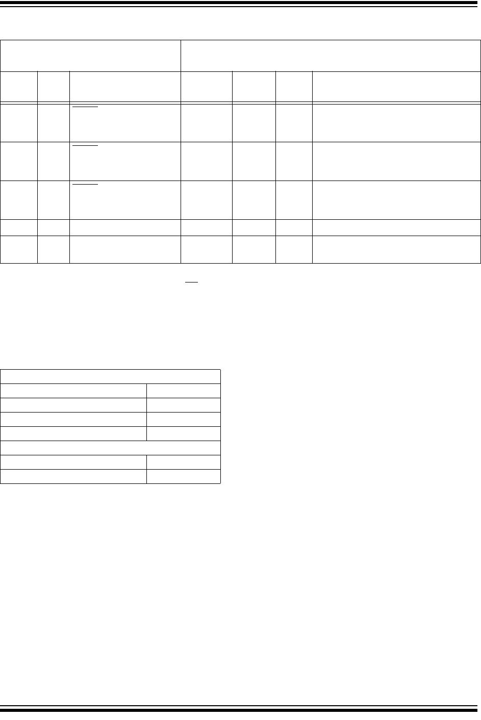
2.2 Read Sequence
The device is selected by pulling CS low. The 8-bit
READ instruction is transmitted to the 25XX320A fol-
lowed by the 16-bit address, with the four MSBs of the
address being “don’t care” bits. After the correct READ
instruction and address are sent, the data stored in the
memory at the selected address is shifted out on the
SO pin. The data stored in the memory at the next
address can be read sequentially by continuing to pro-
vide clock pulses. The internal Address Pointer is auto-
matically incremented to the next higher address after
each byte of data is shifted out. When the highest
address is reached (0FFFh), the address counter rolls
over to address 0000h allowing the read cycle to be
continued indefinitely. The read operation is terminated
by raising the CS
pin (Figure 2-1).
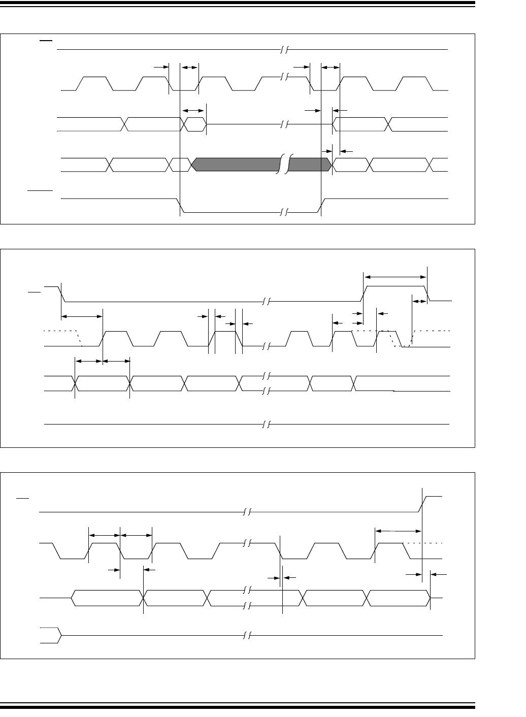
2.3 Write Sequence
Prior to any attempt to write data to the 25XX320A, the
write enable latch must be set by issuing the WREN
instruction (Figure 2-4). This is done by setting CS
low
and then clocking out the proper instruction into the
25XX320A. After all eight bits of the instruction are
transmitted, the CS
must be brought high to set the
write enable latch. If the write operation is initiated
immediately after the WREN instruction without CS
being brought high, the data will not be written to the
array because the write enable latch will not have been
properly set.
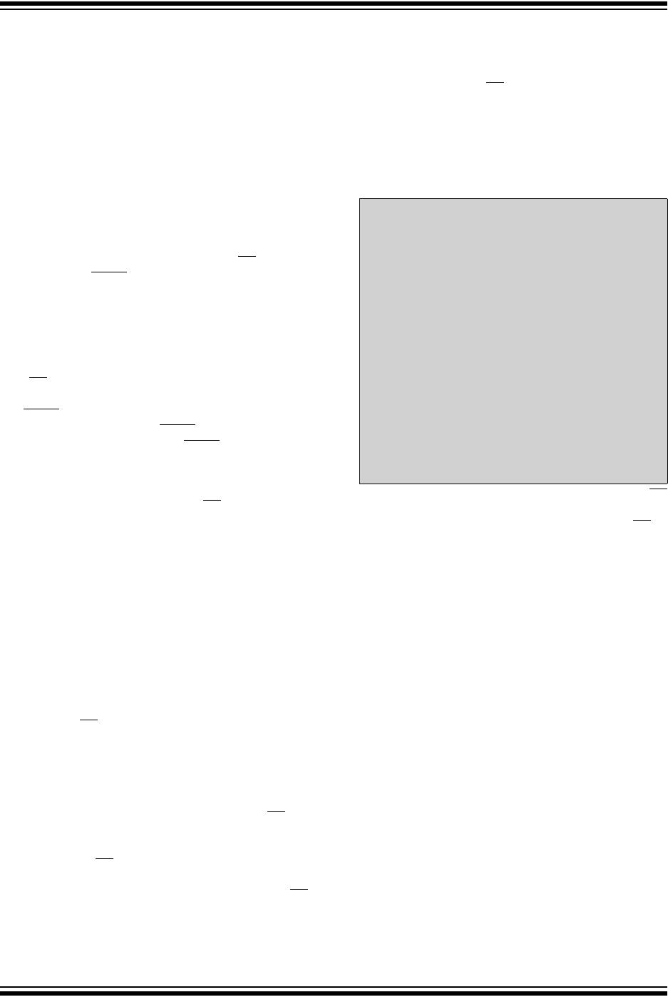
Once the write enable latch is set, the user may
proceed by setting the CS low, issuing a WRITE instruc-
tion, followed by the 16-bit address, with the four MSBs
of the address being “don’t care” bits, and then the data
to be written. Up to 32 bytes of data can be sent to the
device before a write cycle is necessary. The only
restriction is that all of the bytes must reside in the
same page.
For the data to be actually written to the array, the CS
must be brought high after the Least Significant bit (D0)
of the n
th
data byte has been clocked in. If CS is
brought high at any other time, the write operation will
not be completed. Refer to Figure 2-2 and Figure 2-3
for more detailed illustrations on the byte write
sequence and the page write sequence, respectively.
While the write is in progress, the STATUS register may
be read to check the status of the WPEN, WIP, WEL,
BP1 and BP0 bits (Figure 2-6). A read attempt of a
memory array location will not be possible during a
write cycle. When the write cycle is completed, the
write enable latch is reset.
Note: Page write operations are limited to writing
bytes within a single physical page,
regardless of the number of bytes
actually being written. Physical page
boundaries start at addresses that are
integer multiples of the page buffer size (or
‘page size’) and, end at addresses that are
integer multiples of page size – 1. If a
Page Write command attempts to write
across a physical page boundary, the
result is that the data wraps around to the
beginning of the current page (overwriting
data previously stored there), instead of
being written to the next page as might be
expected. It is therefore necessary for the
application software to prevent page write
operations that would attempt to cross a
page boundary.