LTC4370
13
4370f
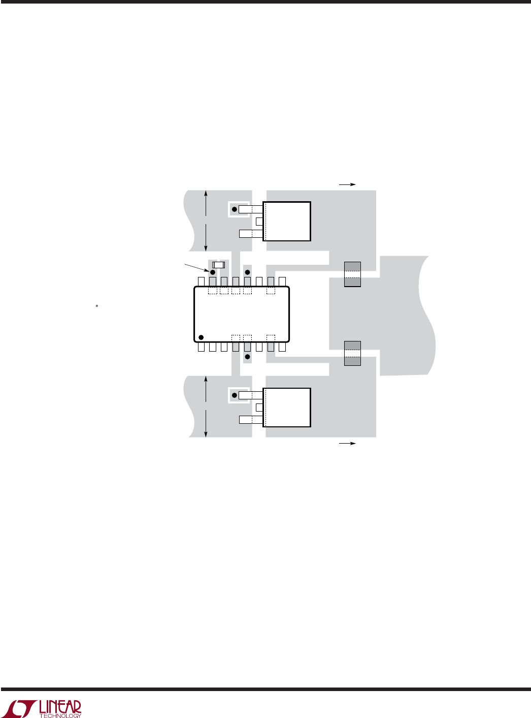
External CPO Supply
The internal charge pump takes milliseconds to charge
up the CPO capacitor especially during device power-up.
This time can be shortened by connecting an external
supply to the CPO pin. A series resistor is needed to limit
the current into the internal clamp between the CPO and
V
IN
pins. The CPO supply should also be higher than the
main input supply to meet the gate drive requirements
of the MOSFET. Figure 5 shows such a 3.3V load share
application, where a 12V supply is connected to the CPO
pins through a 1k resistor. The 1k limits the current into
the CPO pin when the V
IN
pin is grounded. For the 8.7V
of gate drive (12V – 3.3V), logic-level MOSFETs would be
an appropriate choice for M1 and M2.
Loop Stability
The servo amplifier loop is compensated by the gate
capacitance of the N-channel power MOSFET. No further
compensation components are normally required. In the
case when a MOSFET with less than 1nF gate capacitance
is chosen, a 1nF compensation capacitor connected across
the gate and source might be required.
The load sharing control loop is compensated by the
capacitor from the COMP pin to ground. This
capacitor
should
be at least 50× the input capacitance C
ISS
of the
MOSFET. A larger capacitor improves stability at the ex-
pense of increased sharing closure delay, while a smaller
capacitor can cause the two supply currents to switch back
and forth before settling. The COMP capacitor can be just
10× C
ISS
when a CPO capacitor is omitted, i.e., when fast
gate turn-on is not used (see Figure 6).
Input and Output Capacitance for Pulsed Loads
For pulsed loads, the load current will be shared every cycle
at frequencies below 100Hz. At higher frequencies, each
cycle’s current may not be shared but the time average of
the currents will be. Bypassing capacitance on the inputs
should be provided to minimize glitches and ripple. This
is important since the controller tries to compensate for
the supply voltage differences to achieve load sharing.
Sufficient load capacitance should also be provided to
enhance the DC component of the load current presented
to the load share circuit. It is also important to design
I
L
• R
DS(ON)
below 75mV, as mentioned earlier.
With very low duty cycle or very low frequency loads,
the COMP voltage will rail whenever the load
current falls
below
the sharing threshold of V
EA(OS)
/R
S
for hundreds of
milliseconds. At the start of the next load cycle there will
be a sharing closure delay as COMP slews to its operating
point around 0.7V or 1.24V. To avoid this delay, maintain
the load current above V
EA(OS)
/R
S
.
Figure 5. 3.3V Load Share with External 12V Supply
Powering CPO for Faster Start-Up and Refresh
GATE1
CPO1
CPO2
4370 F05
V
INA
3.3V
V
INB
3.3V
12V
1k
1k
TO SENSE
RESISTOR
TO SENSE
RESISTOR
M1
M2
C1
39nF
C2
39nF
V
IN1
GATE2V
IN2
LTC4370
applicaTions inForMaTion
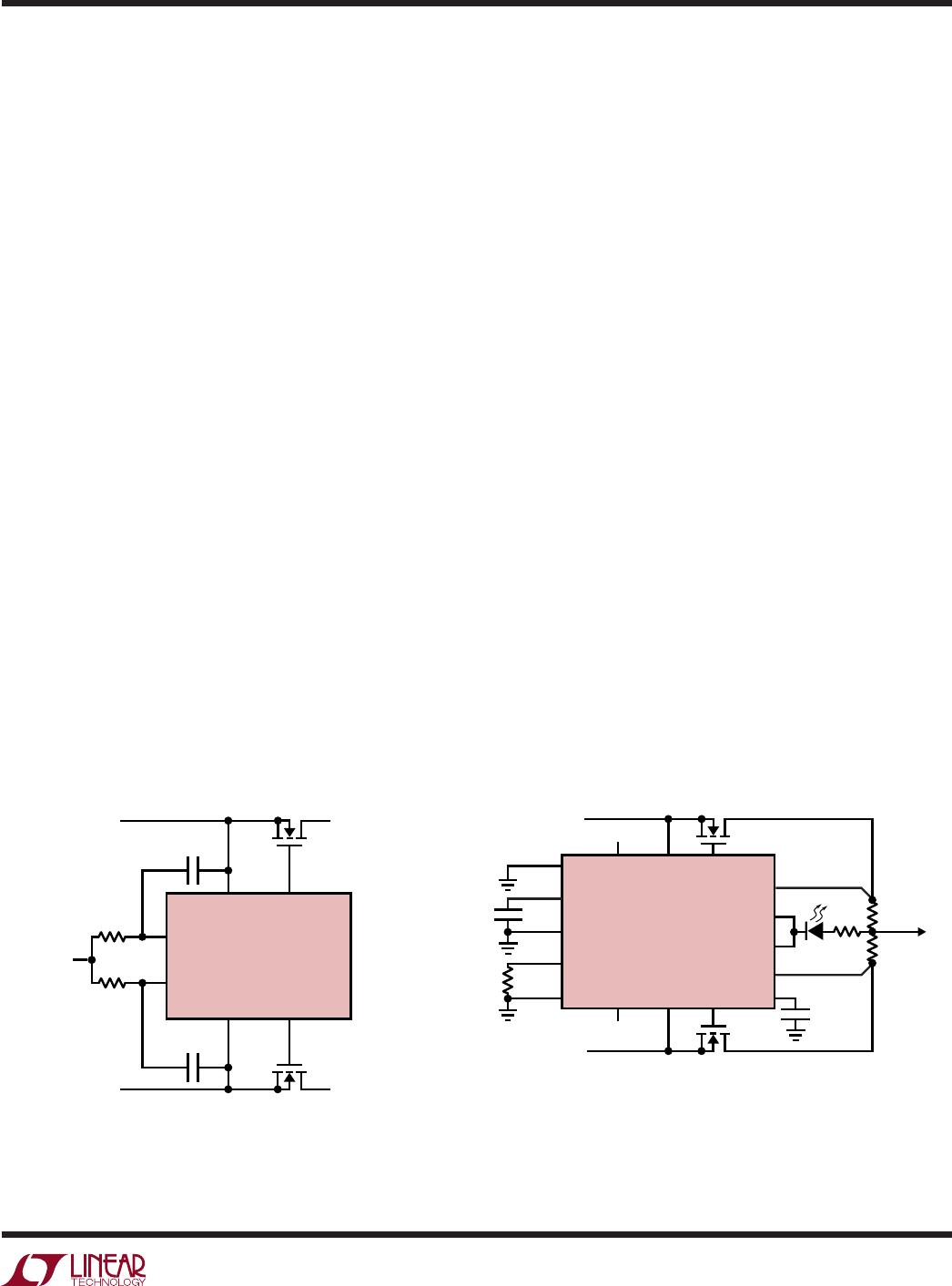
Figure 6. Current Sharing 12V Supplies
M2
SUM85N03-06P D1: RED LED, LN1251C
NC
NC
D1
M1
SUM85N03-06P
GATE1CPO1
CPO2
GND
EN1
EN2
RANGE
4370 F06
V
INA
12V
V
INB
12V
OUT
10A
V
IN1
V
CC
FETON1
COMP
FETON2
OUT1
OUT2
GATE2
V
IN2
LTC4370
R1
2.5mΩ
R2
2.5mΩ
C
C
0.039µF
C
VCC
0.1µF
R3
47.5k
R4
2.7k