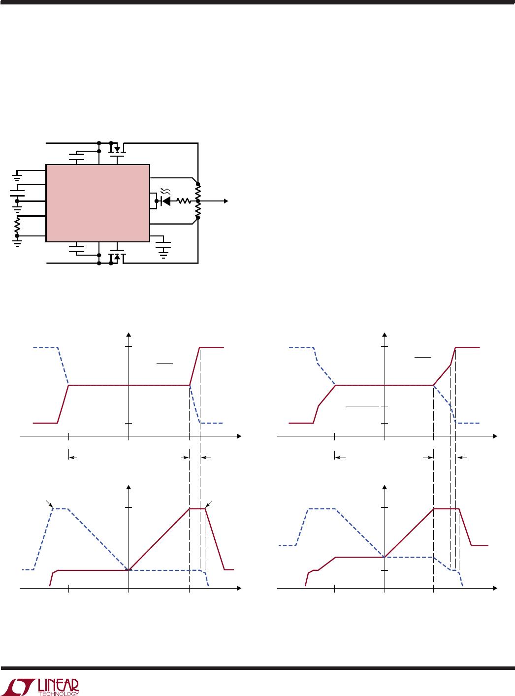
LTC4370
7
4370f
FuncTional DiagraM
4370 BD
CHARGE
PUMP1
f = 3MHz
LDO
CHARGE
PUMP2
f = 3MHz
*DE PACKAGE ONLY
GATE1
OFF
GATE2
OFF
+
SA1
+
+
+
+
11
CPO1
12
GATE1
13
V
IN1
V
CC
V
CC
V
CC
LOW
V
IN1
g
m
= 150µS
V
IN2
V
IN1
V
FR1
V
FR2
V
CC
V
SUPPLY1
10
9
OUT1
FETON1
500k
CP4
CP2
CP1
CP3
CP5
0.7V
0.6V
0.6V
2.55V
0.3V
COMP
GATE1
OUT1
OUT2
RANGE
CPO2GATE2
17
EXPOSED
PAD*
GND V
IN2
OUT2
M1
V
SUPPLY2
M2
+
C1
C2
DISABLE
LOAD SHARE
DISABLE1
DISABLE2
+
+
+
V
CC
V
IN2
8
FETON2
1
EN2
14
V
CC
16
EN1
500k
CP6
0.7V
GATE2
C
C
10µA
TO
LOAD
R3
C
VCC
Z
R1
R2
SERVO
ADJUST
3
2
6515 4 7
SA2
EA
+
+
+
+
+
LTC4370
8
4370f
operaTion
The LTC4370 controls N-channel MOSFETs, M1 and M2,
to share the load between two supplies. Error amplifier
EA compares OUT1 to OUT2 and sets the servo com-
mand voltages, V
FR1
and V
FR2
, for servo amplifiers, SA1
and SA2. When enabled, each servo amplifier controls
the gate of the external MOSFET to regulate its forward
voltage drop (V
FWD
= V
IN
OUT) to V
FR
. The combined
action of EA and SA forces OUT1 to equal OUT2. Having
the power path resistance from OUT1 to the load (R1)
equal that from OUT2 to the load (R2) forces each supply
to source half of the load current.
The lower limit of V
FR
adjustment is 25mV at higher supply
voltages (reducing to 12mV at lower voltages to conserve
power and voltage drop). The upper limit is V
RANGE
+ 25mV
(or V
RANGE
+ 12mV). V
RANGE
itself is set by the 10µA pull-
up current source into resistor R3. The servo adjust block
ensures that only the higher supply’s V
FR
is adjusted up
while the other is pinned to the minimum. Tying RANGE to
V
CC
(CP5) forces both V
FR
to the minimum, transforming
the device into a dual ideal diode controller.
The
servo amplifier raises the gate voltage to enhance
the MOSFET whenever the load current causes the drop
to exceed V
FR
. For large output currents the MOSFET
gate is driven fully on and the voltage drop is equal to
I
FET
R
DS(ON)
.
In the case of an input supply short-circuit, when the
MOSFET is conducting, a large reverse current starts
flowing from the load towards the input. SA detects this
failure condition as soon as it appears and turns off the
MOSFET by rapidly pulling down its gate.
SA quickly pulls up the gate whenever it senses a large
forward voltage drop. An external capacitor (C1, C2)
between the CPO and V
IN
pins is needed for fast gate
pull-up. This capacitor is charged up, at device power-up,
by the internal charge-pump. The stored charge is used
for the fast gate pull-up.
The GATE pin sources current from the CPO pin and sinks
current to the V
IN
and GND pins. Clamps limit the GATE
and CPO voltages to 12V above and a diode below V
IN
.
Internal switches pull the FETON pins low when the GATE
to V
IN
voltage is below 0.7V to indicate that the external
MOSFET is off (body diode could still conduct).
LDO is a low dropout regulator that generates a 5V supply
at the V
CC
pin from the highest V
IN
input. When supplies
below 2.9V are being shared, an external supply in the
2.9V to 6V range is required at the V
CC
pin.
V
CC
and EN pin comparators, CP1 to CP3, control power
passage. The MOSFET is held off whenever the EN pin is
above 0.6V, or the V
CC
pin is below 2.55V. A high on both
EN pins lowers the current consumption of the device.
LTC4370
9
4370f
High availability systems often employ parallel-connected
power supplies or battery feeds to achieve redundancy
and enhance system reliability. ORing diodes have been
a popular means of connecting these supplies at the point
of load. System uptime improves further if these paralleled
supplies also share the load current.
applicaTions inForMaTion
Figure 1. 5V Diode-OR Load Share with Status Light
Current Sharing Characteristic
The LTC4370 load shares the two supplies by dropping
their voltage difference across the MOSFETs in series
with them (see Figure 1). The MOSFET on the lower sup-
ply drops the minimum servo voltage V
FR(MIN)
(12mV
or 25mV depending on supply voltage levels), while the
other MOSFET drops V
FR(MIN)
plus the supply voltage
difference. This equalizes both the OUT pin voltages, and
by Ohm’s law the current that flows through the sense
resistors. Figure2a illustrates this. It shows the higher
supply’s MOSFET forward voltage drop, V
FWD
, increasing
to compensate the supply difference up to ±500mV.
The upper limit of the servo command adjustment is the
minimum servo plus the RANGE pin voltage (500mV in
Figure 2). Hence, when the two supplies differ by a volt-
age equal to V
RANGE
, the higher supply’s V
FWD
is pinned
at the maximum servo voltage V
FR(MAX)
. If the supplies
diverge by more than V
RANGE
, the OUT pin voltages start
Figure 2. Load Sharing Characteristics
4370 F02
(2b) High R
DS(ON)
: Fully-On MOSFET
Drops 125mV at Half Load
–400mV 400mV0
525mV
25mV
MOSFET
FORWARD
DROP
V
IN1
– V
IN2
V
FWD1
V
FWD2
0.5I
L
• R
DS(ON)
125mV
100mV + I
L
• R
S
–400mV 400mV0
1
0
NORMALIZED
CURRENT
V
IN1
– V
IN2
I
2
I
1
I
1
I
2
0.5
SHARING CAPTURE RANGE
±∆V
IN(SH)
DRAWING IS NOT TO SCALE!
V
FR(MIN)
I
L
• R
DS(ON)
2R
S
+ R
DS(ON)
(2a) Low R
DS(ON)
: Can Servo 25mV Minimum
Forward Regulation Voltage at Half Load
–500mV 500mV0
525mV
25mV
MOSFET
FORWARD
DROP
MAXIMUM M2
MOSFET POWER
DISSIPATION
V
IN1
– V
IN2
V
FWD1
V
FWD2
V
FR(MAX)
V
FR(MIN)
I
L
• R
S
–500mV 500mV0
1
0
NORMALIZED
CURRENT
V
IN1
– V
IN2
I
2
I
1
I
1
I
2
0.5
SHARING CAPTURE RANGE ±∆V
IN(SH)
V
RANGE
= 500mV V
RANGE
= 500mV
= 2R
S
1
SLOPE
= 2R
S
1
SLOPE
MAXIMUM M1
MOSFET POWER
DISSIPATION
M2
SUM85N03-06P
D1: RED LED
LN1251C
SHARE
OFF
D1
M1
SUM85N03-06P
C2
39nF
GATE1CPO1
CPO2
GND
EN1
EN2
RANGE
4370 F01
V
INA
5V
V
INB
5V
C
VCC
0.1µF
R3
30.1k
R4
820Ω
C1
39nF
V
IN1
V
CC
FETON1
COMP
FETON2
OUT1
OUT2
GATE2V
IN2
LTC4370
R1
2.5mΩ
R2
2.5mΩ
OUT
10A
C
C
0.18µF

LTC4370IMS#PBF

Mfr. #:
Manufacturer:
Analog Devices Inc.
Description:
Power Management Specialized - PMIC Two-S Diode-OR C Balancing Cntr
Lifecycle:
New from this manufacturer.
Delivery:
DHL FedEx Ups TNT EMS
Payment:
T/T Paypal Visa MoneyGram Western Union