74AVC2T45_Q100 All information provided in this document is subject to legal disclaimers. © NXP B.V. 2013. All rights reserved.
Product data sheet Rev. 2 — 15 February 2013 14 of 23
NXP Semiconductors
74AVC2T45-Q100
Dual-bit, dual-supply voltage level translator/transceiver; 3-state
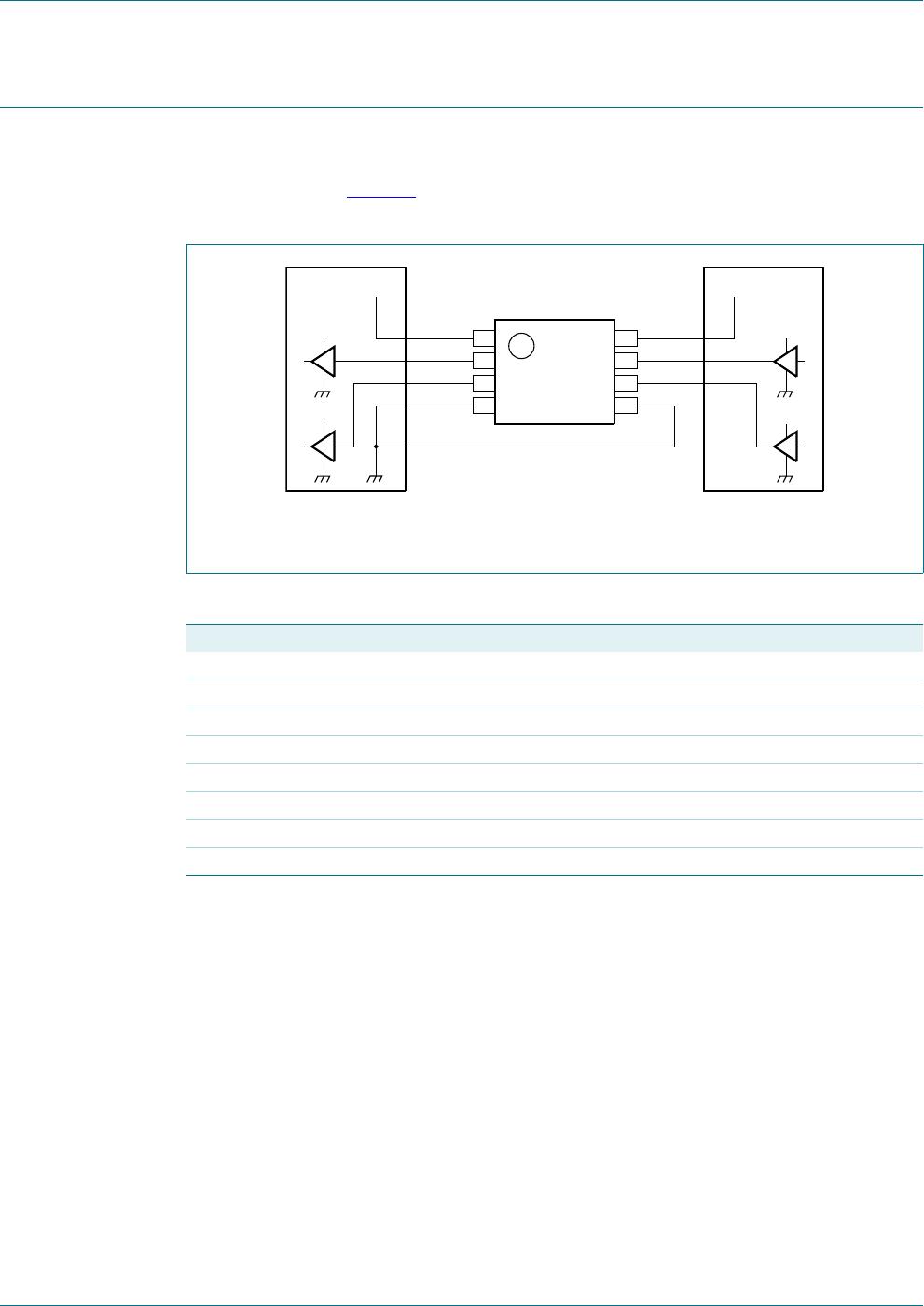
13. Application information
13.1 Unidirectional logic level-shifting application
The circuit given in Figure 8 is an example of the 74AVC2T45-Q100 being used in a
unidirectional logic level-shifting application.
Fig 8. Unidirectional logic level-shifting application
Table 16. Unidirectional logic level-shifting application
Pin Name Function Description
1V
CC(A)
V
CC1
supply voltage of system-1 (0.8 V to 3.6 V)
2 1A OUT1 output level depends on V
CC1
voltage
3 2A OUT2 output level depends on V
CC1
voltage
4 GND GND device GND
5 DIR DIR the GND (LOW level) determines B port to A port direction
6 2B IN2 input threshold value depends on V
CC2
voltage
7 1B IN1 input threshold value depends on V
CC2
voltage
8V
CC(B)
V
CC2
supply voltage of system-2 (0.8 V to 3.6 V)
$9&74
9
&&$
9
&&
9
&&
9
&&
9
&&
9
&&%
$
V\VWHP
%
$ %
*1' ',5
DDD
V\VWHP
9
&&
9
&&

