WM1824B Production Data
w
PD, Rev 4.0, November 2012
10
AUDIO INTERFACE TIMING
Figure 2 Digital Audio Data Timing – Slave Mode
Test Conditions
LINEVDD=AVDD=DBVDD=2.97~3.63V, LINEGND=AGND=0V, T
A
=+25
°
C, Slave Mode
PARAMETER SYMBOL MIN TYP MAX UNIT
Audio Data Input Timing Information
BCLK cycle time
t
BCY
27 ns
BCLK pulse width high
t
BCH
11 ns
BCLK pulse width low
t
BCL
11 ns
LRCLK set-up time to BCLK rising edge
t
LRSU
7 ns
LRCLK hold time from BCLK rising edge
t
LRH
5 ns
DACDAT hold time from LRCLK rising edge
t
DH
5 ns
DACDAT set-up time to BCLK rising edge
t
DS
7 ns
Table 1 Slave Mode Audio Interface Timing
Note:
BCLK period should always be greater than or equal to MCLK period.
Figure 3 Recommended BCLK Transition Area for Optimum Performance
It is recommended that for optimum SNR performance the BCLK transition occurs centred around the
MCLK rising edge, in the region ‘x’ shown in Figure 3 above. Operation out with this region can result
in up to 8dB of degradation in SNR.
Production Data WM1824B
w
PD, Rev 4.0, November 2012
11
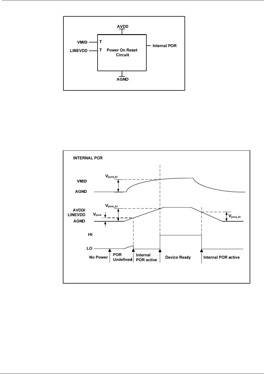
POWER ON RESET CIRCUIT
Figure 4 Internal Power on Reset Circuit Schematic
The WM1824B includes an internal Power-On-Reset circuit, as shown in Figure 4, which is
used to reset the DAC digital logic into a default state after power up. The POR circuit is
powered by AVDD and has as its inputs VMID and LINEVDD. It asserts POR low if VMID or
LINEVDD are below a minimum threshold.
Figure 5 Typical Power Timing Requirements
Figure 5 shows a typical power-up sequence where LINEVDD comes up with AVDD. When
AVDD goes above the minimum threshold, V
pora
, there is enough voltage for the circuit to
guarantee POR is asserted low and the chip is held in reset. In this condition, all writes to the
control interface are ignored. After VMID rises to V
pord_hi
and AVDD rises to V
pora_hi,
POR is
released high and access to the control interface and audio interface may take place. This
assumes that DBVDD is at a level within the recommended operating conditions.
On power down, PORB is asserted low whenever LINEVDD or AVDD drop below the
minimum threshold V
pora_low
.
WM1824B Production Data
w
PD, Rev 4.0, November 2012
12
Test Conditions
LINEVDD = AVDD = DBVDD = 3.3V AGND = LINEGND = 0V, T
A
= +25
o
C
PARAMETER SYMBOL TEST CONDITIONS MIN TYP MAX UNIT
Power Supply Input Timing Information
VDD level to POR defined
(LINEVDD/AVDD rising)
V
pora
Measured from AGND 158 mV
VDD level to POR rising edge
(VMID rising)
V
pord_hi
Measured from AGND 0.63 0.8 1 V
VDD level to POR rising edge
(LINEVDD/AVDD rising)
V
pora_hi
Measured from AGND 1.44 1.8 2.18 V
VDD level to POR falling edge
(LINEVDD/AVDD falling)
V
pora_lo
Measured from AGND 0.96 1.46 1.97 V
Table 2 Power on Reset
Note: All values are simulated results

WM1824BGEDT/R

Mfr. #:
Manufacturer:
Cirrus Logic
Description:
Audio D/A Converter ICs Stereo DAC w/ 2Vrms ground ref line Dvr
Lifecycle:
New from this manufacturer.
Delivery:
DHL FedEx Ups TNT EMS
Payment:
T/T Paypal Visa MoneyGram Western Union

Products related to this Datasheet