XC2C256 CoolRunner-II CPLD
8 www.xilinx.com DS094 (v3.2) March 8, 2007
Product Specification
R
(
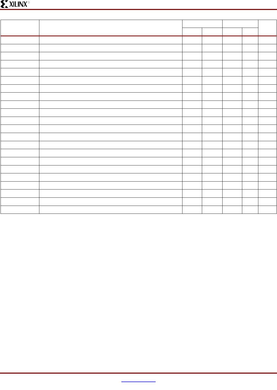
Internal Timing Parameters
Symbol Parameter
(2)
-6 -7
UnitsMin. Max. Min. Max.
Buffer Delays
T
IN
Input buffer delay - 2.4 - 2.6 ns
T
DIN
Direct data register input delay - 3.1 - 3.9 ns
T
GCK
Global Clock buffer delay - 1.8 - 2.7 ns
T
GSR
Global set/reset buffer delay - 2.0 - 3.5 ns
T
GTS
Global 3-state buffer delay - 2.1 - 3.0 ns
T
OUT
Output buffer delay - 2.3 - 2.6 ns
T
EN
Output buffer enable/disable delay - 3.5 - 4.0 ns
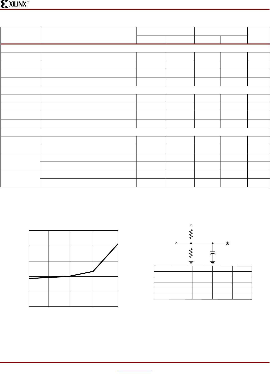
P-term Delays
T
CT
Control term delay - 1.1 - 1.4 ns
T
LOGI1
Single P-term delay adder - 0.5 - 1.1 ns
T
LOGI2
Multiple P-term delay adder - 0.3 - 0.5 ns
Macrocell Delay
T
PDI
Input to output valid - 0.5 - 0.7 ns
T
SUI
Setup before clock 1.3 - 1.8 - ns
T
HI
Hold after clock 0 - 0 - ns
T
ECSU
Enable clock setup time 0.8 - 1.8 - ns
T
ECHO
Enable clock hold time 0 - 0 - ns
T
COI
Clock to output valid - 0.4 - 0.7 ns
T
AOI
Set/reset to output valid - 1.4 - 1.5 ns
T
CDBL
Clock doubler delay - 0 - 0 ns
Feedback Delays
T
F
Feedback delay - 1.7 - 3.0 ns
T
OEM
Macrocell to global OE delay - 1.7 - 2.5 ns
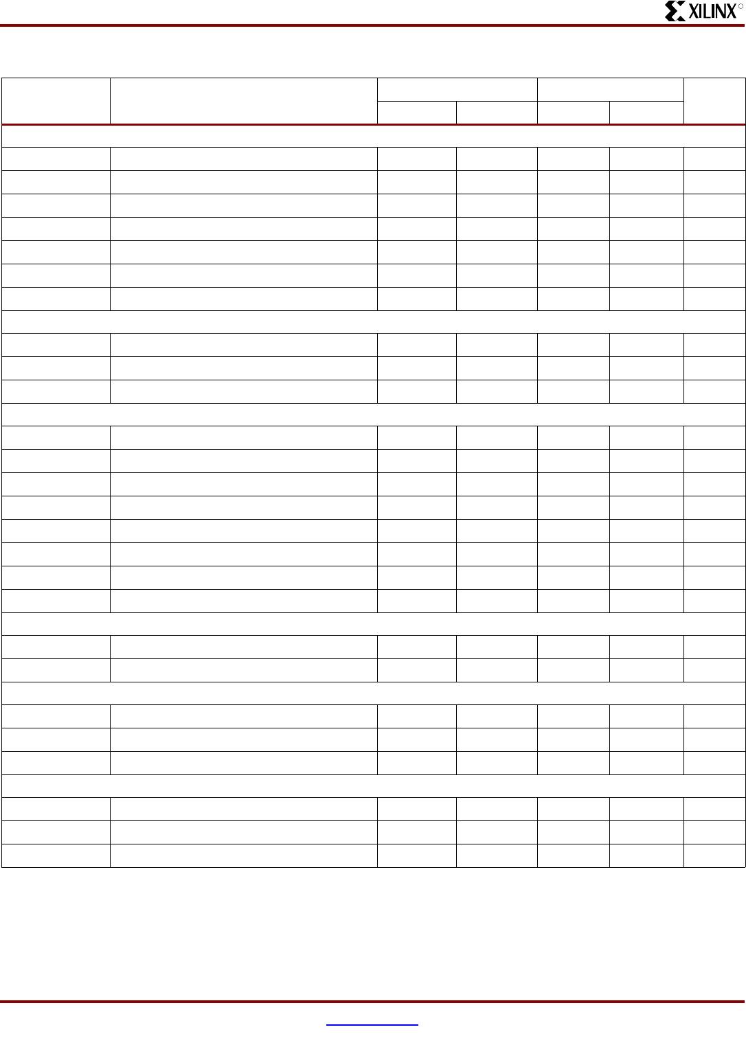
I/O Standard Time Adder Delays 1.5V CMOS
T
HYS15
Hysteresis input adder - 3.0 - 4.0 ns
T
OUT15
Output adder - 0.8 - 1.0 ns
T
SLEW15
Output slew rate adder - 4.0 - 5.0 ns
I/O Standard Time Adder Delays 1.8V CMOS
T
HYS18
Hysteresis input adder - 2.0 - 3.0 ns
T
OUT18
Output adder - 0 - 0 ns
T
SLEW
Output slew rate adder - 2.0 - 4.0 ns