AD7398/AD7399
Rev. C | Page 4 of 24
Parameter Symbol Condition 3 V to 5 V ± 10% ±5 V ± 10% Unit
SUPPLY CHARACTERISTICS
Shutdown Supply Current I
DD_SD
No load 30/60 30/60 μA typ/max
Positive Supply Current I
DD
V
IL
= 0 V, no load, −40°C < T
A
< +125°C 1.5/2.8 1.6/3 mA typ/max
I
DD
V
IL
= 0 V, no load, −40°C < T
A
< +85°C 1.5/2.6 1.6/2.8 mA typ/max
Negative Supply Current I
SS
V
IL
= 0 V, no load 1.5/2.5 1.6/2.7 mA typ/max
Power Dissipation P
DISS
V
IL
= 0 V, no load 5 16 mW typ
Power Supply Sensitivity PSS ΔV
DD
= ±5% 0.006 0.006 %/% max
1
One LSB = V
REF
/4096 V for the 12-bit AD7398.
2
The first eight codes (000
H
to 007
H
) are excluded from the linearity error measurement in single-supply operation.
3
These parameters are guaranteed by design and not subject to production testing.
4
When V
REF
is connected to either the V
DD
or the V
SS
power supply, the corresponding V
OUT
voltage programs between ground and the supply voltage minus the offset
voltage of the output buffer, which is the same as the V
ZSE
error specification. See additional information in the Theory of Operation section.
5
Input resistance is code dependent.
6
Typicals represent average readings measured at 25°C.
7
All input control signals are specified with t
R
= t
F
= 2 ns (10% to 90% of 3 V) and timed from a voltage level of 1.5 V.
8
The settling time specification does not apply for negative going transitions within the last 3 LSBs of ground.
AD7399 10-BIT VOLTAGE OUTPUT DAC
V
DD
= 5 V, V
SS
= 0 V; or V
DD
= + 5 V, V
SS
= –5 V; V
REF
= +2.5 V, −40°C < T
A
< +125°C, unless otherwise noted.
Table 2.
Parameter Symbol Condition 3 V to 5 V ± 10% ±5 V ± 10% Unit
STATIC PERFORMANCE
Resolution
1
N 10 10 Bits
Relative Accuracy
2
INL ±1 ±1 LSB max
Differential Nonlinearity
2
DNL Monotonic ±1 ±1 LSB max
Zero-Scale Error V
ZSE
Data = 000
H
7 ±4 mV max
Full-Scale Voltage Error V
FSE
Data = 3FF
H
±15 ±15 mV max
Full-Scale Tempco
3
TCV
FS
1.5 1.5 ppm/°C typ
REFERENCE INPUT
V
REF
IN Range
4
V
REF
0/V
DD
V
SS
/V
DD
V min/max
Input Resistance
5
R
REF
Data = 155
H
, worst case 40 40 kΩ typ
6
Input Capacitance
3
C
REF
5 5 pF typ
ANALOG OUTPUT
Output Voltage Range V
OUT
0 to V
REF
0 to V
REF
V
Output Current I
OUT
Data = 200
H
, ΔV
OUT
= 1 LSB ±5 ±5 mA typ
Capacitive Load
3
C
L
No oscillation 200 400 pF max
LOGIC INPUTS
Logic Input Low Voltage V
IL
V
DD
= 3 V 0.5 V max
V
DD
= 5 V 0.8 0.8 V max
Logic Input High Voltage V
IH
CLK only 80% V
DD
4.0 V min
2.1 to 2.4 2.4 V min
Input Leakage Current I
IL
1 1 μA max
Input Capacitance
3
C
IL
10 10 pF max
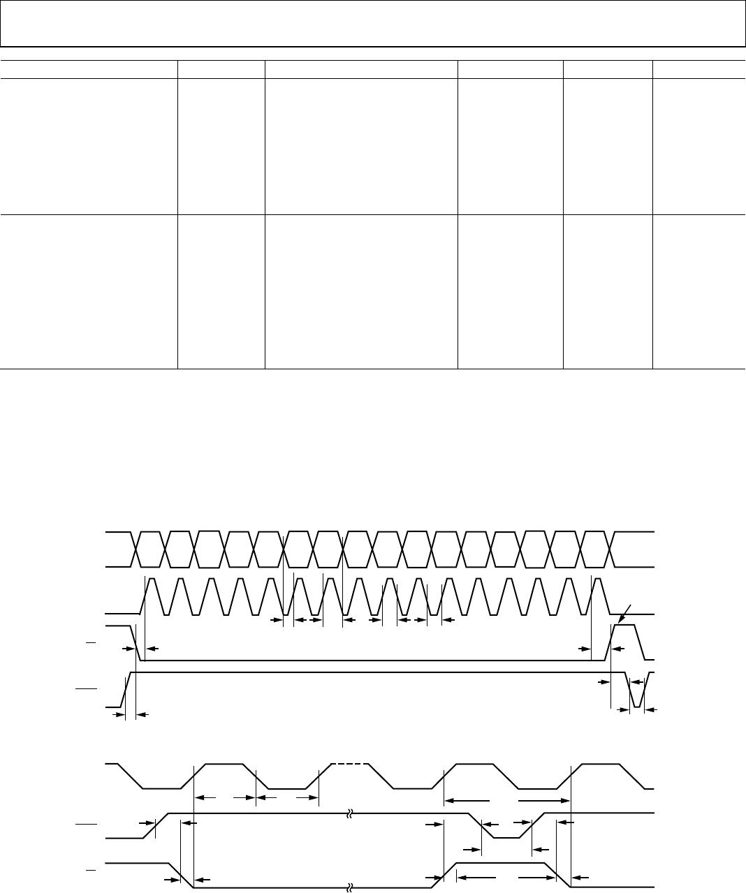
INTERFACE TIMING
3, 7
Clock Frequency f
CLK
11 16.6 MHz max
Clock Width High t
CH
45 30 ns min
Clock Width Low t
CL
45 30 ns min
CS to Clock Setup
t
CSS
10 5 ns min
Clock to CS Hold
t
CSH
20 15 ns min
Load DAC Pulse Width t
LDAC
45 30 ns min
Data Setup t
DS
15 10 ns min
Data Hold t
DH
10 5 ns min
Load Setup to CS
t
LDS
0 0 ns min
Load Hold to CS
t
LDH
20 15 ns min