DATASHEET
5PB11xx MARCH 28, 2017 1 ©2017 Integrated Device Technology, Inc.
1.8V to 3.3V LVCMOS High Performance
Clock Buffer Family
5PB11xx
Description
The 5PB11xx is a high-performance LVCMOS Clock Buffer
Family. It has best-in-class additive phase jitter of 50fsec
RMS.
There are five different fan-out variations, 1:2 to 1:10,
available.
The IDT5PB11xx also supports a synchronous glitch-free
Output Enable function to eliminate any potential intermediate
incorrect output clock cycles when enabling or disabling
outputs. It comes in various packages and can operate from a
1.8V to 3.3V supply.
Features
High performance 1:2, 1:4, 1:6, 1:8, 1:10 LVCMOS clock
buffer
Very low pin-to-pin skew < 50ps
Very low additive jitter < 50fs
Supply voltage: 1.8V to 3.3V
fMAX = 200MHz
Integrated serial termination for 50 channel
Packaged in 8-, 14-, 16-, 20-pin TSSOP and as small as
2 × 2 mm DFN and QFN packages
Industrial (-40°C to +85°C) and extended (-40°C to
+105°C) temperature ranges
Block Diagram
LVCMOS
Y0CLKIN
Y1
Y2
Y3
LVCMOS
LVCMOS
LVCMOS
LVCMOS
LVCMOS
Yn
1G
1.8V TO 3.3V LVCMOS HIGH PERFORMANCE CLOCK BUFFER FAMILY 2 MARCH 28, 2017
5PB11xx DATASHEET
Pin Assignments for TSSOP Packages
Pin Descriptions for TSSOP Packages
Device Number
LVCMOS
Clock Input
Clock Output
Enable
LVCMOS Clock Output Supply Voltage Ground
CLKIN 1G Y0, Y1, . . . Y9 V
DD GND
5PB1102PGG 1 2 3, 8 6 4
5PB1104PGG 1 2 3, 8, 5, 7 6 4
5PB1106PGG 1 2 3, 14, 11, 13, 6, 9 5, 8, 12 4, 7, 10
5PB1108PGG 1 2 3, 16, 13, 15, 6, 11, 8, 9 5, 10, 14 4, 7, 12
5PB1110PGG 1 2 3, 20, 17, 19, 6, 15, 8, 13, 12, 10 5, 9, 14, 18 4, 7, 11, 16
CLKIN
1
2
3
45
6
7
8
1G
Y0
GND
NC
VDD
NC
Y1
5PB1102PGG
CLKIN
1
2
3
45
6
7
8
1G
Y0
GND
Y2
VDD
Y3
Y1
5PB1104PGG
CLKIN
1
2
3
4
5
6
78
9
10
11
12
13
14
1G
Y0
GND
VDD
Y4
GND
VDD
Y5
GND
Y2
VDD
Y3
Y1
5PB1106PGG
CLKIN
1
2
3
4
5
6
7
89
10
11
12
13
14
15
16
1G
Y0
GND
VDD
Y4
GND
Y6
Y7
VDD
Y5
GND
Y2
VDD
Y3
Y1
5PB1108PGG
CLKIN
1
2
3
4
5
6
7
8
9
10 11
12
13
14
15
16
17
18
19
20
1G
Y0
GND
VDD
Y4
GND
Y6
VDD
Y9
GND
Y8
Y7
VDD
Y5
GND
Y2
VDD
Y3
Y1
5PB1110PGG
MARCH 28, 2017 3 1.8V TO 3.3V LVCMOS HIGH PERFORMANCE CLOCK BUFFER FAMILY
5PB11xx DATASHEET
Pin Assignments for DFN/QFN Packages
Pin Descriptions for DFN/QFN Packages
Output Logic Table
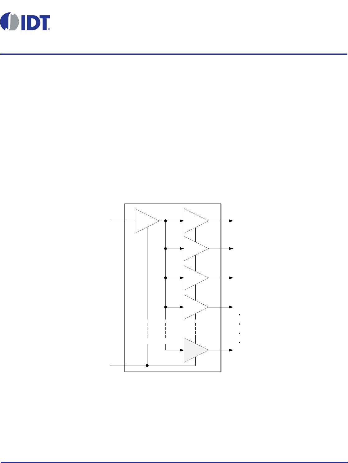
After at least three cycles of input clock toggling. Output Enable function is asynchronous to eliminate any intermediate incorrect output clock cycles during transition which may cause
frequency peaking to the downstream device.
Device Number
LVCMOS
Clock Input
Clock Output
Enable
LVCMOS Clock Output Supply Voltage Ground
CLKIN 1G Y0, Y1, . . . Y9 V
DD GND
5PB1102CMG 1 2 3, 8 6 4
5PB1104CMG 1 2 3, 5, 7, 8 6 4
5PB1106CMG 15 16 1, 4, 9, 11, 13, 14 3, 8, 12 2, 5, 10
5PB1108CMG 15 16 1, 4, 6, 7, 9, 11, 13, 14 3, 8, 12 2, 5, 10
5PB1110NDG 19 20 1, 4, 6, 8, 10, 11, 13, 15, 17, 18 3, 7, 12, 16 2, 5, 9, 14
Inputs Output
CLKIN 1G Yn
XLL
LHL
HHH
CLKIN
1
2
3
45
6
7
8
1G
Y0
GND
NC
VDD
NC
Y1
5PB1102CMG
CLKIN
1
2
3
45
6
7
8
1G
Y0
GND
Y2
VDD
Y3
Y1
5PB1104CMG
CLKIN
1
2
3
4
5
678
9
10
11
12
13
14
1516
1G
Y0
GND
VDD
Y4
GND
Y6
Y5
VDD
Y2
GND
VDD
Y3
Y1
5PB1108CMG
Y7
CLKIN
1
2
3
4
5
678910
11
12
13
14
15
1617181920
1G
Y0
GND
VDD
Y4
GND
Y6
VDD
Y9
GND
Y8
Y7
VDD
Y5
GND
Y2
VDD
Y3
Y1
5PB1110NDG

5PB1110NDGI

Mfr. #:
Manufacturer:
IDT
Description:
Clock Buffer 1.8V to 3.3V LVCMOS 200MHz 5,9,14,18 VDD
Lifecycle:
New from this manufacturer.
Delivery:
DHL FedEx Ups TNT EMS
Payment:
T/T Paypal Visa MoneyGram Western Union