LT1167
12
1167fc
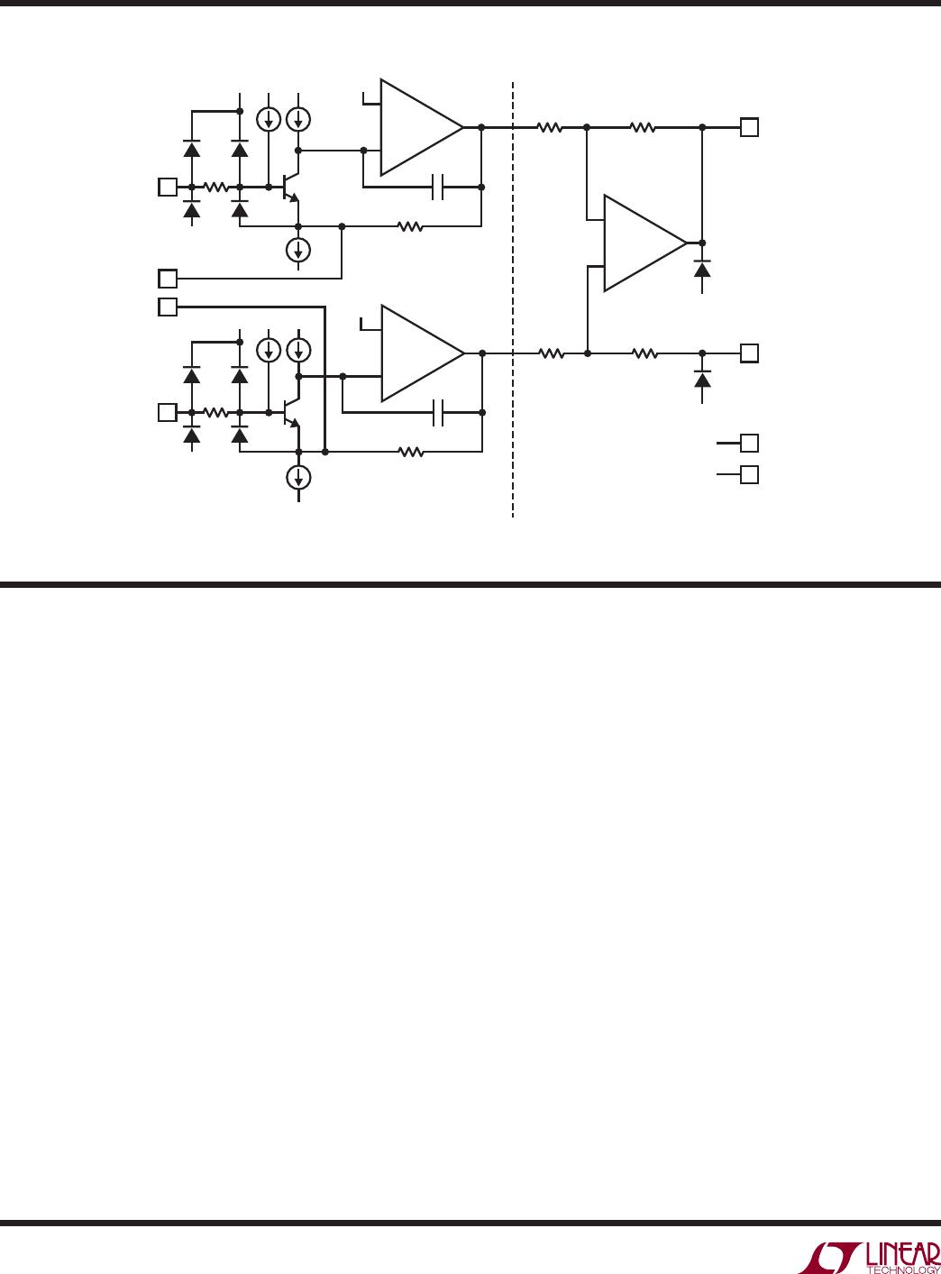
BLOCK DIAGRAM
THEORY OF OPERATION
Q1
R
G
2
OUTPUT
6
REF
1167 F01
5
7
–
+
A1
–
+
A3
VB
R1
24.7k
R3
400Ω
R4
400Ω
C1
1
R
G
8
R7
10k
R8
10k
R5
10k
R6
10k
DIFFERENCE AMPLIFIER STAGEPREAMP STAGE
+IN
–IN
3
–
+
A2
VB
R2
24.7k
C2
V
+
V
–
V
–
V
+
V
–
Q2 V
–
V
+
4
V
–
Figure 1. Block Diagram
The LT1167 is a modified version of the three op amp
instrumentation amplifier. Laser trimming and mono-
lithic construction allow tight matching and tracking of
circuit parameters over the specified temperature range.
Refer to the block diagram (Figure 1) to understand the
following circuit description. The collector currents in
Q1 and Q2 are trimmed to minimize offset voltage drift,
thus assuring a high level of performance. R1 and R2 are
trimmed to an absolute value of 24.7k to assure that the
gain can be set accurately (0.05% at G = 100) with only
one external resistor R
G
. The value of R
G
determines the
transconductance of the preamp stage. As R
G
is reduced
for larger programmed gains, the transconductance of
the input preamp stage increases to that of the input
transistors Q1 and Q2. This increases the open-loop gain
when the programmed gain is increased, reducing the
input referred gain related errors and noise. The input
voltage noise at gains greater than 50 is determined only
by Q1 and Q2. At lower gains the noise of the difference
amplifier and preamp gain setting resistors increase the
noise. The gain bandwidth product is determined by C1,
C2 and the preamp transconductance which increases
with programmed gain. Therefore, the bandwidth does
not drop proportionally to gain.
The input transistors Q1 and Q2 offer excellent matching,
which is inherent in NPN bipolar transistors, as well as
picoampere input bias current due to superbeta process-
ing. The collector currents in Q1 and Q2 are held constant
due to the feedback through the Q1-A1-R1 loop and
Q2-A2-R2 loop which in turn impresses the differential
input voltage across the external gain set resistor R
G
. Since
the current that flows through R
G
also flows through R
1
and R2, the ratios provide a gained-up differential voltage,
G = (R1 + R2)/R
G
, to the unity-gain difference
amplifier A3.
The common mode voltage is removed by A3, resulting
in a single-ended output voltage referenced to the voltage
on the REF pin. The resulting gain equation is:
V
OUT
– V
REF
= G(V
IN
+
– V
IN
–
)
where:
G = (49.4kΩ/R
G
) + 1
solving for the gain set resistor gives:
R
G
= 49.4kΩ/(G – 1)