LT1167
13
1167fc
THEORY OF OPERATION
Input and Output Offset Voltage
The offset voltage of the LT1167 has two components:
the output offset and the input offset. The total offset
voltage referred to the input (RTI) is found by dividing the
output offset by the programmed gain (G) and adding it
to the input offset. At high gains the input offset voltage
dominates, whereas at low gains the output offset voltage
dominates. The total offset voltage is:
Total input offset voltage (RTI)
= input offset + (output offset/G)
Total output offset voltage (RTO)
= (input offset • G) + output offset
Reference Terminal
The reference terminal is one end of one of the four 10k
resistors around the difference amplifier. The output volt-
age of the LT1167 (Pin 6) is referenced to the voltage on
the reference terminal (Pin 5). Resistance in series with
the REF pin must be minimized for best common mode
rejection. For example, a 2Ω resistance from the REF pin
to ground will not only increase the gain error by 0.02%
but will lower the CMRR to 80dB.
Single Supply Operation
For single supply operation, the REF pin can be at the
same potential as the negative supply (Pin 4) provided the
output of the instrumentation amplifier remains inside the
specified operating range and that one of the inputs is at
least 2.5V above ground. The barometer application on
the front page of this data sheet is an example that satis-
fies these conditions. The resistance R
b
from the bridge
transducer to ground sets the operating current for the
bridge and also has the effect of raising the input common
mode voltage. The output of the LT1167 is always inside
the specified range since the barometric pressure rarely
goes low enough to cause the output to rail (30.00 inches
of Hg corresponds to 3.000V). For applications that require
the output to swing at or below the REF potential, the
voltage on the REF pin can be level shifted. An op amp is
used to buffer the voltage on the REF pin since a parasitic
series resistance will degrade the CMRR. The application
in the back of this data sheet, Four Digit Pressure Sensor,
is an example.
Output Offset Trimming
The LT1167 is laser trimmed for low offset voltage so that
no external offset trimming is required for most applica-
tions. In the event that the offset needs to be adjusted, the
circuit in Figure 2 is an example of an optional offset adjust
circuit. The op amp buffer provides a low impedance to
the REF pin where resistance must be kept to minimum
for best CMRR and lowest gain error.
+
2
–IN
OUTPUT
+IN
1
8
10k
100Ω
100Ω
–10mV
1167 F02
V
V
+
10mV
5
2
3
1
6
1/2
LT1112
±10mV
ADJUSTMENT RANGE
R
G
3
+
LT1167
REF
Figure 2. Optional Trimming of Output Offset Voltage
Input Bias Current Return Path
The low input bias current of the LT1167 (350pA) and
the high input impedance (200GΩ) allow the use of high
impedance sources without introducing additional offset
voltage errors, even when the full common mode range is
required. However, a path must be provided for the input
bias currents of both inputs when a purely differential
signal is being amplified. Without this path the inputs
will float to either rail and exceed the input common
mode range of the LT1167, resulting in a saturated input
stage. Figure 3 shows three examples of an input bias
current path. The first example is of a purely differential
signal source with a 10kΩ input current path to ground.
Since the impedance of the signal source is low, only one
resistor is needed. Two matching resistors are needed for
higher impedance signal sources as shown in the second
example. Balancing the input impedance improves both
common mode rejection and DC offset. The need for input
resistors is eliminated if a center tap is present as shown
in the third example.
LT1167
14
1167fc
APPLICATIONS INFORMATION
THEORY OF OPERATION
10k
R
G
R
G
R
G
1167 F03
THERMOCOUPLE
200k
MICROPHONE,
HYDROPHONE,
ETC
200k
CENTER-TAP PROVIDES
BIAS CURRENT RETURN
+
LT1167
+
LT1167
+
LT1167
Figure 3. Providing an Input Common Mode Current Path
The LT1167 is a low power precision instrumentation
amplifier that requires only one external resistor to accu-
rately set the gain anywhere from 1 to 1000. The output
can handle capacitive loads up to 1000pF in any gain
configuration and the inputs are protected against ESD
strikes up to 13kV (human body).
Input Current at High Common Mode Voltage
When operating within the specified input common mode
range, both the LT1167 and LT1167-1 operate as shown
in the Input Bias Current vs Common Mode Input Voltage
graph shown in the Typical Performance Characteristics.
If however the inputs are within approximately 0.8V of
the positive supply, the LT1167 input current will increase
to approximately –1μA to –3μA. If the impedance of the
circuit driving the LT1167 inputs is sufficiently high (e.g.,
10MΩ when +V
S
= 15V), this increased input current can
pull the input voltage sufficiently high to keep the elevated
input current flowing. The LT1167-1 has been modified so
that the input current is typically two orders of magnitude
lower under similar conditions. The LT1167-1 is recom-
mended for new designs where input impedance is high.
Input Protection
The LT1167 can safely handle up to ±20mA of input cur-
rent in an overload condition. Adding an external 5k input
resistor in series with each input allows DC input fault
voltages up to ±100V and improves the ESD immunity
to 8kV (contact) and 15kV (air discharge), which is the
IEC 1000-4-2 level 4 specification. If lower value input
resistors are needed, a clamp diode from the positive supply
to each input will maintain the IEC 1000-4-2 specification
to level 4 for both air and contact discharge. A 2N4393
drain/source to gate is a good low leakage diode for use
with 1k resistors, see Figure 4. The input resistors should
be carbon and not metal film or carbon film.
V
EE
1167 F04
V
CC
V
CC
V
CC
J2
2N4393
J1
2N4393
OUT
OPTIONAL FOR HIGHEST
ESD PROTECTION
R
G
R
IN
R
IN
+
LT1167
REF
Figure 4. Input Protection
RFI Reduction
In many industrial and data acquisition applications,
instrumentation amplifiers are used to accurately amplify
small signals in the presence of large common mode volt-
ages or high levels of noise. Typically, the sources of these
very small signals (on the order of microvolts or millivolts)
are sensors that can be a significant distance from the
signal conditioning circuit. Although these sensors may be
connected to signal conditioning circuitry, using shielded
or unshielded twisted-pair cabling, the cabling may act
as antennae, conveying very high frequency interference
directly into the input stage of the LT1167.
LT1167
15
1167fc
APPLICATIONS INFORMATION
The amplitude and frequency of the interference can have
an adverse effect on an instrumentation amplifiers input
stage by causing an unwanted DC shift in the amplifiers
input offset voltage. This well known effect is called RFI
rectification and is produced when out-of-band interference
is coupled (inductively, capacitively or via radiation) and
rectified by the instrumentation amplifiers input transis-
tors. These transistors act as high frequency signal detec-
tors, in the same way diodes were used as RF envelope
detectors in early radio designs. Regardless of the type
of interference or the method by which it is coupled into
the circuit, an out-of-band error signal appears in series
with the instrumentation amplifiers inputs.
To significantly reduce the effect of these out-of-band
signals on the input offset voltage of instrumentation am-
plifiers, simple lowpass filters can be used at the inputs.
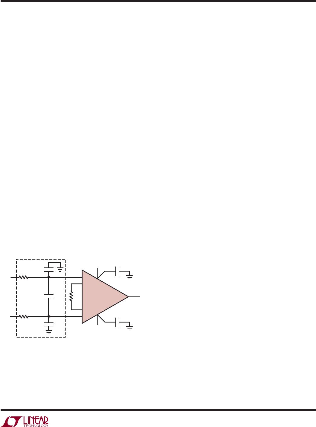
These filters should be located very close to the input pins
of the circuit. An effective filter configuration is illustrated
in Figure 5, where three capacitors have been added to the
inputs of the LT1167. Capacitors C
XCM1
and C
XCM2
form
lowpass filters with the external series resistors R
S1, 2
to any out-of-band signal appearing on each of the input
traces. Capacitor C
XD
forms a filter to reduce any unwanted
signal that would appear across the input traces. An added
benefit to using C
XD
is that the circuit’s AC common mode
rejection is not degraded due to common mode capacitive
imbalance. The differential mode and common mode time
constants associated with the capacitors are:
t
DM(LPF)
= (2)(R
S
)(C
XD
)
t
CM(LPF)
= (R
S1, 2
)(C
XCM1, 2
)
Setting the time constants requires a knowledge of the
frequency, or frequencies of the interference. Once this
frequency is known, the common mode time constants can
be set followed by the differential mode time constant. To
avoid any possibility of inadvertently affecting the signal
to be processed, set the common mode time constant an
order of magnitude (or more) larger than the differential
mode time constant. Set the common mode time constants
such that they do not degrade the LT1167’s inherent AC
CMR. Then the differential mode time constant can be set
for the bandwidth required for the application. Setting the
differential mode time constant close to the sensors BW
also minimizes any noise pickup along the leads. To avoid
any possibility of common mode to differential mode signal
conversion, match the common mode time constants to
1% or better. If the sensor is an RTD or a resistive strain
gauge, then the series resistors R
S1, 2
can be omitted, if the
sensor is in proximity to the instrumentation amplifier.
“Roll Your Own”—Discrete vs Monolithic LT1167
Error Budget Analysis
The LT1167 offers performance superior to that of “roll
your own” three op amp discrete designs. A typical ap-
plication that amplifies and buffers a bridge transducers
differential output is shown in Figure 6. The amplifier, with
its gain set to 100, amplifies a differential, full-scale output
voltage of 20mV over the industrial temperature range. To
make the comparison challenging, the low cost version of
the LT1167 will be compared to a discrete instrumentation
amp made with the A grade of one of the best precision
quad op amps, the LT1114A. The LT1167C outperforms
the discrete amplifier that has lower V
OS
, lower I
B
and
comparable V
OS
drift. The error budget comparison in
Table 1 shows how various errors are calculated and how
each error affects the total error budget. The table shows
the greatest differences between the discrete solution and
V
V
+
IN
+
IN
1167 F05
V
OUT
R
G
C
XCM1
0.001μF
C
XCM2
0.001μF
C
XD
0.1μF
R
S1
1.6k
R
S2
1.6k
EXTERNAL RFI
FILTER
+
LT1167
f
3dB
≈ 500Hz
Figure 5. Adding a Simple RC Filter at the Inputs to an
Instrumentation Amplifier Is Effective in Reducing Rectification
of High Frequency Out-of-Band Signals

LT1167CS8#PBF

Mfr. #:
Manufacturer:
Analog Devices Inc.
Description:
Instrumentation Amplifiers 1x Res Gain Progmable, Prec Instr Amp
Lifecycle:
New from this manufacturer.
Delivery:
DHL FedEx Ups TNT EMS
Payment:
T/T Paypal Visa MoneyGram Western Union