AD7874
REV. C
–13–
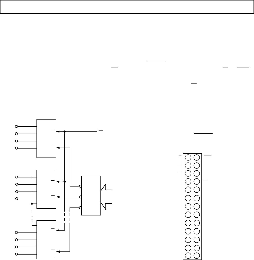
MULTIPLE AD7874s
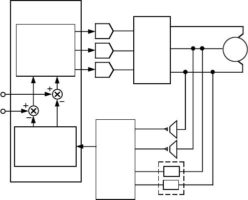
Figure 18 shows a system where a number of AD7874s can be
configured to handle multiple input channels. This type of con-
figuration is common in applications such as sonar, radar, etc.
The AD7874 is specified with maximum and minimum limits on
aperture delay. This means that the user knows the maximum
difference in the sampling instant between all channels. This al-
lows the user to maintain relative phase information between the
different channels.
A common read signal from the microprocessor drives the
RD
input of all AD7874s. Each AD7874 is designated a unique ad-
dress selected by the address decoder. The reference output of
AD7874 number 1 is used to drive the reference input of all
other AD7874s in the circuit shown in Figure 18. One REF
OUT pin can drive several AD7874 REF IN pins. Alternatively,
an external or system reference can be used to drive all REF IN
inputs. A common reference ensures good full-scale tracking be-
tween all channels.
AD7874(1)
AD7874(2)
AD7874(n)
CS
RD
CS
RD
CS
RD
RD
ADDRESS
REF OUT
REF IN
REF IN
ADDRESS
DECODE
V
CH5
V
CH6
V
CH7
V
CH8
V
CH1
V
CH2
V
CH3
V
CH4
V
CHm
V
CHm+1
V
CHm+2
V
CHm+3
Figure 18. Multiple AD7874s in Multichannel System
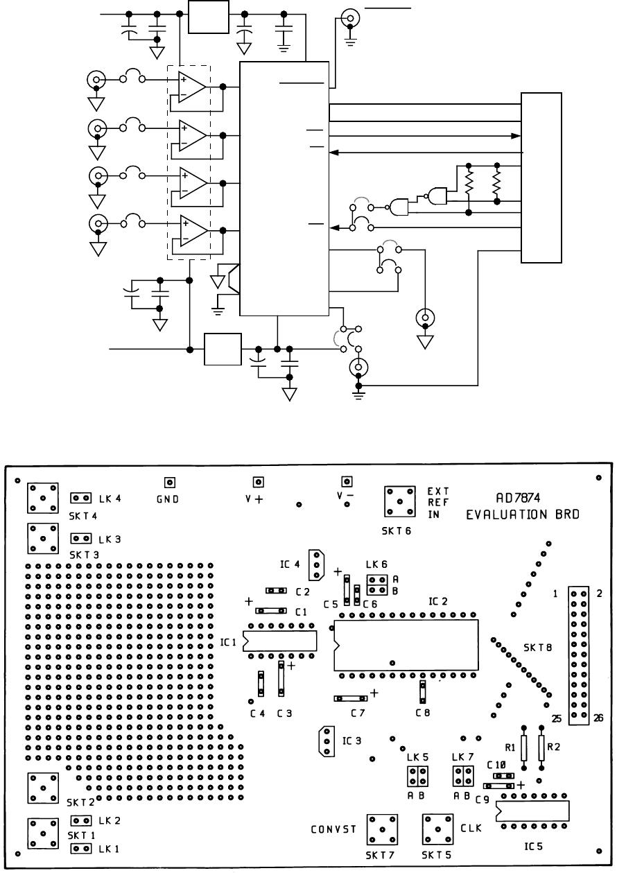
DATA ACQUISITION BOARD
Figure 20 shows the AD7874 in a data acquisition circuit. The
corresponding printed circuit board (PCB) layout and silkscreen
are shown in Figures 21 to 23. A 26-contact IDC connector pro-
vides for a microprocessor connection to the board.
A component grid is provided near the analog inputs on the
PCB which may be used to provide antialiasing filters for the
analog input channels or to provide signal conditioning circuitry.
To facilitate this option, four shorting plugs (labeled LK1 to
LK4 on the PCB) are provided on the analog inputs, one plug
per input. If the shorting plug for a particular channel is used,
the input signal connects to the buffer amplifier driving the ana-
log input of the ADC. If the shorting plug is omitted, a wire link
can be used to connect the input signal to the PCB component
grid.
Microprocessor connections to the board are made via a 26-
contact IDC connector, SKT8, the pinout for which is shown in
Figure 19. This connector contains all data, control and status
signals of the AD7874 (with the exception of the CLK input
and the
CONVST input which are provided via SKT5 and
SKT7, respectively). It also contains decoded R/
W and STRB
inputs which are necessary for TMS32020 interfacing (and also
for 68000 interfacing although pin labels on the 68000 are dif-
ferent). Note that the AD7874
CS input must be decoded prior
to the AD7874 evaluation board.
SKT1, SKT2, SKT3 and SKT4 provide the inputs for V
IN1
,
V
IN2
, V
IN3
, V
IN4
respectively. Assuming LK1 to LK4 are in
place, these input signals are fed to four buffer amplifiers, IC1,
before being applied to the AD7874. The use of an external
clock source is optional; there is a shorting plug (LK5) on the
AD7874 CLK input which must be connected to either –5 V
(for the ADCs own internal clock) or to SKT5. SKT6 and
SKT7 provide the reference and
CONVST inputs respectively.
Shorting plug LK6 provides the option of using the external ref-
erence or the ADCs own internal reference.
DB10
DB8
DB6
DB4
DB2
DB0
GND
R/W
RD
CS
1
3
5
7
9
13
15
17
19
25
23
21
11
N/C
N/C
2
4
6
8
10
14
16
18
20
26
24
22
12
DB11
DB9
DB7
DB5
DB3
DB1
GND
STRB
INT
N/C
N/C
N/C
5V
+
5V
+
Figure 19. SKT8, IDC Connector Pinout
POWER SUPPLY CONNECTIONS
The PCB requires two analog power supplies and one 5 V digi-
tal supply. The analog supplies are labeled V+ and V– and the
range for both supplies is 12 V to 15 V (see silkscreen in Figure
23). Connection to the 5 V digital supply is made via SKT8.
The +5 V supply and the –5 V supply required by the AD7874
are generated from voltage regulators (IC3 and IC4) on the V+
and V– supplies.