AD7874
REV. C
–16–
C1388a–5–5/91
SHORTING PLUG OPTIONS
There are seven shorting plug options which must be set before
using the board. These are outlined below:
LK1–LK4 Connects the analog inputs to the buffer amplifi-
ers. The analog inputs may also be connected to a
component grid for signal conditioning.
LK5 Selects either the AD7874 internal clock or an ex-
ternal clock source.
LK6 Selects either the AD7874 internal reference or an
external reference source.
LK7 Connects the AD7874
RD input directly to the
RD input of SKT8 or to a decoded STRB and
R/
W input. This shorting plug setting depends on
the microprocessor, e.g., the TMS32020 and
68000 require a decoded
RD signal.
COMPONENT LIST
IC1 AD713 Quad Op Amp
IC2 AD7874 Analog-to-Digital Converter
IC3 MC78L05 +5 V Regulator
IC4 MC79L05 –5 V Regulator
IC5 74HC00 Quad NAND Gate
C1, C3, C5, C7, C9 10 µF Capacitors
C2, C4, C6, C8, C10 0.1 µF Capacitors
R1, R2 10 kΩ Pull-Up Resistors
LK1, LK2, LK3 Shorting Plugs
LK4, LK5, LK6
LK7
SKT1, SKT2, SKT3, BNC Sockets
SKT4, SKT5, SKT6,
SKT7
SKT8 26-Contact (2-Row) IDC Connector
PRINTED IN U.S.A.
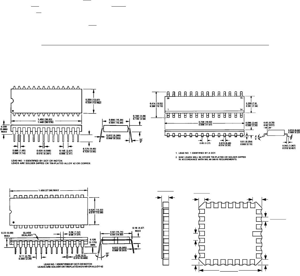
OUTLINE DIMENSIONS
Dimensions shown in inches and (mm).
Plastic (N-28)
Cerdip (Q-28)
SOIC (R-28)
LCCC (E-28A)
0.458 (11.63)
2
0.442 (11.23)
BOTTOM VIEW
NO. 1 PIN INDEX
0.055 (1.40)
0.045 (1.14)
0.028 (0.71)
0.022 (0.56)
0.050 ± 0.005
(1.27 ± 0.13)
0.040 x 45°
(1.02 x 45°)
REF 3 PLCS
0.020 x 45°
(0.51 x 45°) REF
0.100 (2.54)
1
0.064 (1.63)
NOTES
1. THIS DIMENSION CONTROLS THE OVERALL PACKAGE
THICKNESS.
2. APPLIES TO ALL FOUR SIDES.
3. ALL TERMINALS ARE GOLD PLATED.
28
0.075
(1.91)
REF
