AD7874
REV. C
–3–
TIMING CHARACTERISTICS
1
Parameter A, B Versions S Version Units Conditions/Comments
t
1
50 50 ns min CONVST Pulse Width
t
2
0 0 ns min CS to RD Setup Time
t
3
60 70 ns min RD Pulse Width
t
4
0 0 ns min CS to RD Hold Time
t
5
60 60 ns max RD to INT Delay
t
6
2
57 70 ns max Data Access Time after RD
t
7
3
55ns min Bus Relinquish Time after RD
45 50 ns max
t
8
130 150 ns min Delay Time between Reads
t
CONV
31 31 µs min CONVST to INT, External Clock
32.5 32.5 µs max
CONVST to INT, External Clock
31 31 µs min
CONVST to INT, Internal Clock
35 35 µs max
CONVST to INT, Internal Clock
t
CLK
10 10 µs max Minimum Input Clock Period
NOTES
1
Timing Specifications in bold print are 100% production tested. All other times are sample tested at +25°C to ensure compliance. All input signals are specified with
tr = tf = 5 ns (10% to 90% of +5 V) and timed from a voltage level of 1.6 V.
2
t
6
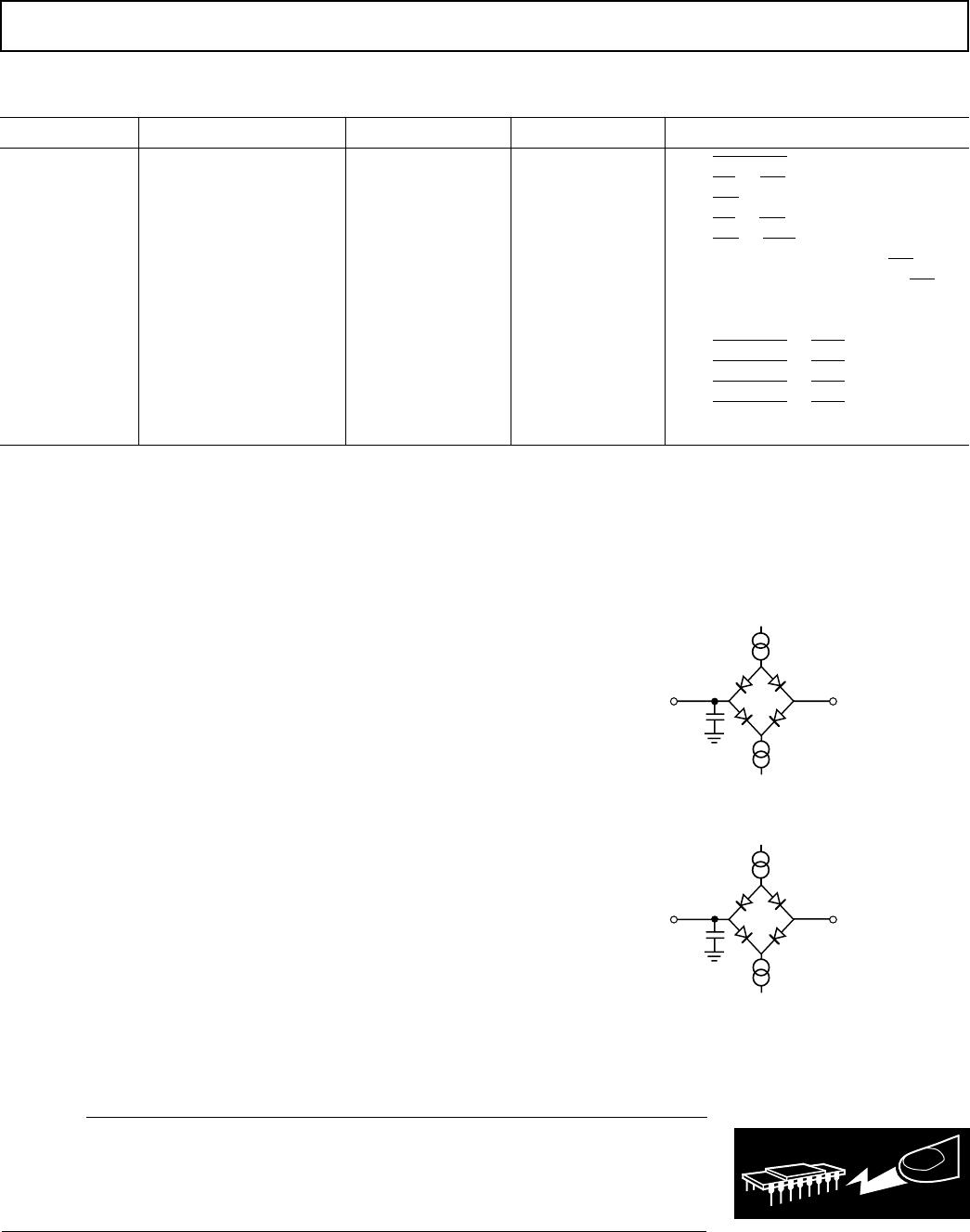
is measured with the load circuit of Figure 1 and defined as the time required for an output to cross 0.8 V or 2.4 V.
3
t
7
is derived from the measured time taken by the data outputs to change 0.5 V when loaded with the circuit of Figure 2. The measured number is then extrapolated
back to remove the effects of charging or discharging the 50 pF capacitor. This means that the time, t
7
, quoted in the timing characteristics is the true bus relinquish
time of the part and as such is independent of external bus loading capacitances.
Specifications subject to change without notice.
(V
DD
= +5 V 6 5%, V
SS
= –5 V 6 5%, AGND = DGND = O V, t
CLK
= 2.5 MHz external unless
otherwise noted.)
ABSOLUTE MAXIMUM RATINGS*
(T
A
= +25°C unless otherwise noted)
V
DD
to AGND . . . . . . . . . . . . . . . . . . . . . . . . . –0.3 V to +7 V
V
DD
to DGND . . . . . . . . . . . . . . . . . . . . . . . . . –0.3 V to +7 V
V
SS
to AGND . . . . . . . . . . . . . . . . . . . . . . . . . +0.3 V to –7 V
AGND to DGND . . . . . . . . . . . . . . . . –0.3 V to V
DD
+ 0.3 V
V
IN
to AGND . . . . . . . . . . . . . . . . . . . . . . . . .–15 V to +15 V
REF OUT to AGND . . . . . . . . . . . . . . . . . . . . . . . 0 V to V
DD
Digital Inputs to DGND . . . . . . . . . . . –0.3 V to V
DD
+ 0.3 V
Digital Outputs to DGND . . . . . . . . . . –0.3 V to V
DD
+ 0.3 V
Operating Temperature Range
Commercial (A, B Versions) . . . . . . . . . . . –40°C to +85°C
Extended (S Version) . . . . . . . . . . . . . . . . –55°C to +125°C
Storage Temperature Range . . . . . . . . . . . . –65°C to +150°C
Lead Temperature (Soldering, 10 secs) . . . . . . . . . . . +300°C
Power Dissipation (Any Package) to +75°C . . . . . . 1,000 mW
Derates above +75°C by . . . . . . . . . . . . . . . . . . . . 10 mW/°C
*Stresses above those listed under “Absolute Maximum Ratings” may cause
permanent damage to the device. This is a stress rating only and functional
operation of the device at these or any other conditions above those listed in the
operational sections of this specifications is not implied. Exposure to absolute
maximum rating conditions for extended periods may affect device reliability.
TO OUTPUT
PIN
1.6mA
2.1V+
200µA
50pF
Figure 1. Load Circuit for Access Time
TO OUTPUT
PIN
1.6mA
2.1V+
200µA
50pF
Figure 2. Load Circuit for Bus Relinquish Time
WARNING!
ESD SENSITIVE DEVICE
CAUTION
ESD (electrostatic discharge) sensitive device. Electrostatic charges as high as 4000 V readily
accumulate on the human body and test equipment and can discharge without detection.
Although the AD7874 features proprietary ESD protection circuitry, permanent damage may
occur on devices subjected to high energy electrostatic discharges. Therefore, proper ESD
precautions are recommended to avoid performance degradation or loss of functionality.
AD7874
REV. C
–4–
TERMINOLOGY
ACQUISITION TIME
Acquisition Time is the time required for the output of the
track/hold amplifiers to reach their final values, within ±1/2
LSB, after the falling edge of
INT (the point at which the track/
holds return to track mode). This includes switch delay time,
slewing time and settling time for a full-scale voltage change.
APERTURE DELAY
Aperture Delay is defined as the time required by the internal
switches to disconnect the hold capacitors from the inputs. This
produces an effective delay in sample timing. It is measured by
applying a step input and adjusting the
CONVST input position
until the output code follows the step input change.
APERTURE DELAY MATCHING
Aperture Delay Matching is the maximum deviation in aperture
delays across the four on-chip track/hold amplifiers.
APERTURE JITTER
Aperture Jitter is the uncertainty in aperture delay caused by
internal noise and variation of switching thresholds with signal
level.
DROOP RATE
Droop Rate is the change in the held analog voltage resulting
from leakage currents.
CHANNEL-TO-CHANNEL ISOLATION
Channel-to-Channel Isolation is a measure of the level of
crosstalk between channels. It is measured by applying a full-
scale 1 kHz signal to the other three inputs. The figure given is
the worst case across all four channels.
SNR, THD, IMD
See DYNAMIC SPECIFICATIONS section.
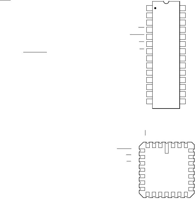
PIN CONFIGURATIONS
DIP and SOIC
V
IN1
V
IN2
V
IN4
V
IN3
REF IN
AGND
DB0 (LSB)
V
DD
V
SS
REF OUT
CLK DB1
V
DD
DB2
DB11 (MSB) DB3
DB10 DB4
DB9 DB5
DB8 DB6
DGND DB7
13
18
1
2
28
27
5
6
7
24
23
22
3
4
26
25
821
920
10
19
1111
12
17
16
14
15
TOP VIEW
(Not to Scale)
AD7874
INT
CONVST
RD
CS
LCCC
V
DD
CLK
V
DD
V
IN4
V
IN2
V
IN1
DB9
DB8
DB6
DGND
DB7
REF OUT
REF IN
DB1
AGND
DB0 (LSB)
DB10
DB11 (MSB)
DB4
DB5
V
SS
V
IN3
DB3
DB2
AD7874
27
1
2822634
25
22
24
23
21
19
20
181712 13 1614 15
11
10
9
8
7
6
5
TOP VIEW
(Not to Scale)
CONVST
RD
CS
INT
AD7874
REV. C
–5–
PIN FUNCTION DESCRIPTION
Pin Mnemonic Description
1V
IN1
Analog Input Channel 1. This is the first of the four input channels to be converted in a con-
version cycle. Analog input voltage range is ±10 V.
2V
IN2
Analog Input Channel 2. Analog input voltage range is ±10 V.
3V
DD
Positive supply voltage, +5 V ± 5%. This pin should be decoupled to AGND.
4
INT Interrupt. Active low logic output indicating converter status. See Figure 7.
5
CONVST Convert Start. Logic Input. A low to high transition on this input puts the track/hold into its
hold mode and starts conversion. The four channels are converted sequentially, Channel 1 to
Channel 4. The
CONVST input is asynchronous to CLK and independent of CS and RD.
6
RD Read. Active low logic input. This input is used in conjunction with CS low to enable the
data outputs. Four successive reads after a conversion will read the data from the four chan-
nels in the sequence, Channel 1, 2, 3, 4.
7
CS Chip Select. Active low logic input. The device is selected when this input is active.
8 CLK Clock Input. An external TTL-compatible clock may be applied to this input pin. Alterna-
tively, tying this pin to V
SS
enables the internal laser trimmed clock oscillator.
9V
DD
Positive Supply Voltage, +5 V ± 5%. Same as Pin 3; both pins must be tied together at the
package. This pin should be decoupled to DGND.
10 DB11 Data Bit 11 (MSB). Three-state TTL output. Output coding is 2s complement.
11–13 DB10–DB8 Data Bit 10 to Data Bit 8. Three-state TTL outputs.
14 DGND Digital Ground. Ground reference for digital circuitry.
15–21 DB7–DB1 Data Bit 7 to Data Bit 1. Three-state TTL outputs.
22 DB0 Data Bit 0 (LSB). Three-state TTL output.
23 AGND Analog Ground. Ground reference for track/hold, reference and DAC.
24 REF IN Voltage Reference Input. The reference voltage for the part is applied to this pin. It is inter-
nally buffered, requiring an input current of only ±1 µA. The nominal reference voltage for
correct operation of the AD7874 is 3 V.
25 REF OUT Voltage Reference Output. The internal 3 V analog reference is provided at this pin. To oper-
ate the AD7874 with internal reference, REF OUT is connected to REF IN. The external
load capability of the reference is 500 µA.
26 V
SS
Negative Supply Voltage, –5 V ± 5%.
27 V
IN3
Analog Input Channel 3. Analog input voltage range is ±10 V.
28 V
IN4
Analog Input Channel 4. Analog input voltage range is ±10 V.
ORDERING GUIDE
Relative
Temperature SNR Accuracy Package
Model
1
Range (dBs) (LSB) Option
2
AD7874AN –40°C to +85°C 70 min ±1 max N-28
AD7874BN –40°C to +85°C 72 min ±1/2 max N-28
AD7874AR –40°C to +85°C 70 min ±1 max R-28
AD7874BR –40°C to +85°C 72 min ±1/2 max R-28
AD7874AQ –40°C to +85°C 70 min ±1 max Q-28
AD7874BQ –40°C to +85°C 72 min ±1/2 max Q-28
AD7874SQ
3
–55°C to +125°C 70 min ±1 max Q-28
AD7874SE
3
–55°C to +125°C 70 min ±1 max E-28A
NOTES
1
To order MIL-STD-883, Class B processed parts, add /883B to part number. Contact
1
our local sales office for military data sheet and availability.
2
E = Leaded Ceramic Chip Carrier; N = Plastic DIP; Q = Cerdip; R = SOIC.
3
Available to /883B processing only.

AD7874BNZ

Mfr. #:
Manufacturer:
Analog Devices Inc.
Description:
Analog to Digital Converters - ADC Data Acquisition System IC 12-Bit
Lifecycle:
New from this manufacturer.
Delivery:
DHL FedEx Ups TNT EMS
Payment:
T/T Paypal Visa MoneyGram Western Union