www.vishay.com
10
Document Number: 67344
S11-2380-Rev. C, 28-Nov-11
Vishay Siliconix
SiZ900DT
New Product
This document is subject to change without notice.
THE PRODUCTS DESCRIBED HEREIN AND THIS DOCUMENT ARE SUBJECT TO SPECIFIC DISCLAIMERS, SET FORTH AT www.vishay.com/doc?91000
CHANNEL-2 TYPICAL CHARACTERISTICS (25 °C, unless otherwise noted)
* The power dissipation P
D
is based on T
J(max)
= 150 °C, using junction-to-case thermal resistance, and is more useful in settling the upper
dissipation limit for cases where additional heatsinking is used. It is used to determine the current rating, when this rating falls below the package
limit.
Current Derating*
0
20
40
60
80
100
120
140
0 25 50 75 100 125 150
I
D
- Drain Current (A)
T
C
- Case Temperature (°C)
Package Limited
Power, Junction-to-Case
0
20
40
60
80
100
25 50 75 100 125 150
Power (W)
T
C
- Case Temperature (°C)
Document Number: 67344
S11-2380-Rev. C, 28-Nov-11
www.vishay.com
11
Vishay Siliconix
SiZ900DT
New Product
This document is subject to change without notice.
THE PRODUCTS DESCRIBED HEREIN AND THIS DOCUMENT ARE SUBJECT TO SPECIFIC DISCLAIMERS, SET FORTH AT www.vishay.com/doc?91000
CHANNEL-2 TYPICAL CHARACTERISTICS (25 °C, unless otherwise noted)
Vishay Siliconix maintains worldwide manufacturing capability. Products may be manufactured at one of several qualified locations. Reliability data for Silicon
Technology and Package Reliability represent a composite of all qualified locations. For related documents such as package/tape drawings, part marking, and
reliability data, see www.vishay.com/ppg?67344
.
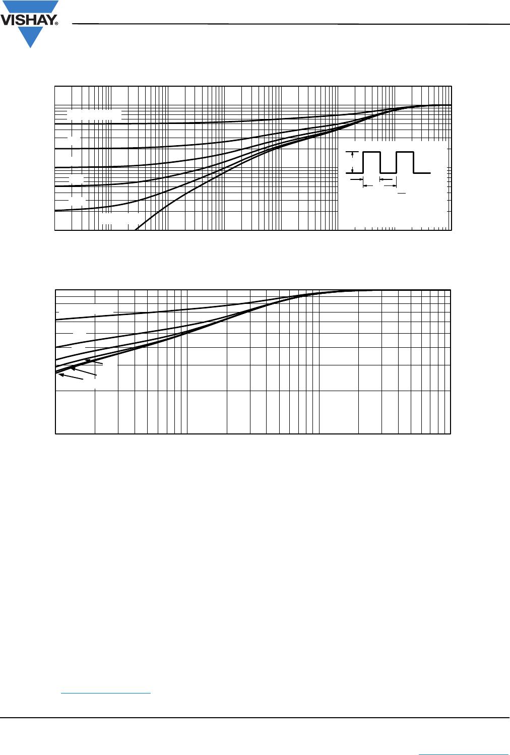
Normalized Thermal Transient Impedance, Junction-to-Ambient
0.01
0.1
1
0.0001 0.001 0.01 0.1 1 10 100 1000
Normalized Effective Transient
Thermal Impedance
Square Wave Pulse Duration (s)
Duty Cycle = 0.5
0.2
0.1
0.05
0.02
Single Pulse
t
1
t
2
Notes:
P
DM
1. Duty Cycle, D =
2. Per Unit Base = R
thJA
= 56 °C/W
3. T
JM
-T
A
=P
DM
Z
thJA
(t)
t
1
t
2
4. Surface Mounted
Normalized Thermal Transient Impedance, Junction-to-Case
0.1
1
0.0001 0.001 0.01 0.1
Normalized Effective Transient
Thermal Impedance
Square Wave Pulse Duration (s)
Duty Cycle = 0.5
0.2
0.1
Single Pulse
0.05
0.02
Package Information
www.vishay.com
Vishay Siliconix
Revision: 31-Oct-11
1
Document Number: 69027
THIS DOCUMENT IS SUBJECT TO CHANGE WITHOUT NOTICE. THE PRODUCTS DESCRIBED HEREIN AND THIS DOCUMENT
ARE SUBJECT TO SPECIFIC DISCLAIMERS, SET FORTH AT www.vishay.com/doc?91000
PowerPAIR
®
6 x 5 BW Case Outline
(for SiZ900DT only)
A1
b1
F
F
E
Pin 1
Pin 2
Pin 3 Pin 4
Pin 8 Pin 7 Pin 6 Pin 5
A
E2
e
E1 K
z
L
D1
b
K1
BACK SIDE VIEW
D1
D
0.10
C
2X
A
0.10 C
0.08 C
Pin #1 Ident
(Optional)
0.10 C
2X
C
Pin 5 Pin 6 Pin 8Pin 7
Pin 1Pin 2Pin 3Pin 4
TOP SIDE VIEW
A3
MILLIMETERS INCHES
DIM. MIN. NOM. MAX. MIN. NOM. MAX.
A 0.70 0.75 0.80 0.028 0.030 0.032
A1 0.00 - 0.10 0.000 - 0.004
A3 0.20 REF 0.008 REF
b 0.51 BSC 0.020 BSC
b1 0.25 BSC 0.010 BSC
D 5.00 BSC 0.197 BSC
D1 3.75 3.80 3.85 0.148 0.150 0.152
E 6.00 BSC 0.236 BSC
E1 2.62 2.67 2.72 0.103 0.105 0.107
E2 0.87 0.92 0.97 0.034 0.036 0.038
e 1.27 BSC 0.005 BSC
K 0.45 TYP. 0.018 TYP.
K1 0.66 TYP. 0.026 TYP.
L 0.43 BSC 0.017 BSC
z 0.34 BSC 0.013 BSC
ECN: C11-1247-Rev. D, 31-Oct-11
DWG: 5978

SIZ900DT-T1-GE3

Mfr. #:
Manufacturer:
Vishay
Description:
MOSFET 2N-CH 30V 24A POWERPAIR
Lifecycle:
New from this manufacturer.
Delivery:
DHL FedEx Ups TNT EMS
Payment:
T/T Paypal Visa MoneyGram Western Union

Products related to this Datasheet