www.vishay.com
4
Document Number: 67344
S11-2380-Rev. C, 28-Nov-11
Vishay Siliconix
SiZ900DT
New Product
This document is subject to change without notice.
THE PRODUCTS DESCRIBED HEREIN AND THIS DOCUMENT ARE SUBJECT TO SPECIFIC DISCLAIMERS, SET FORTH AT www.vishay.com/doc?91000
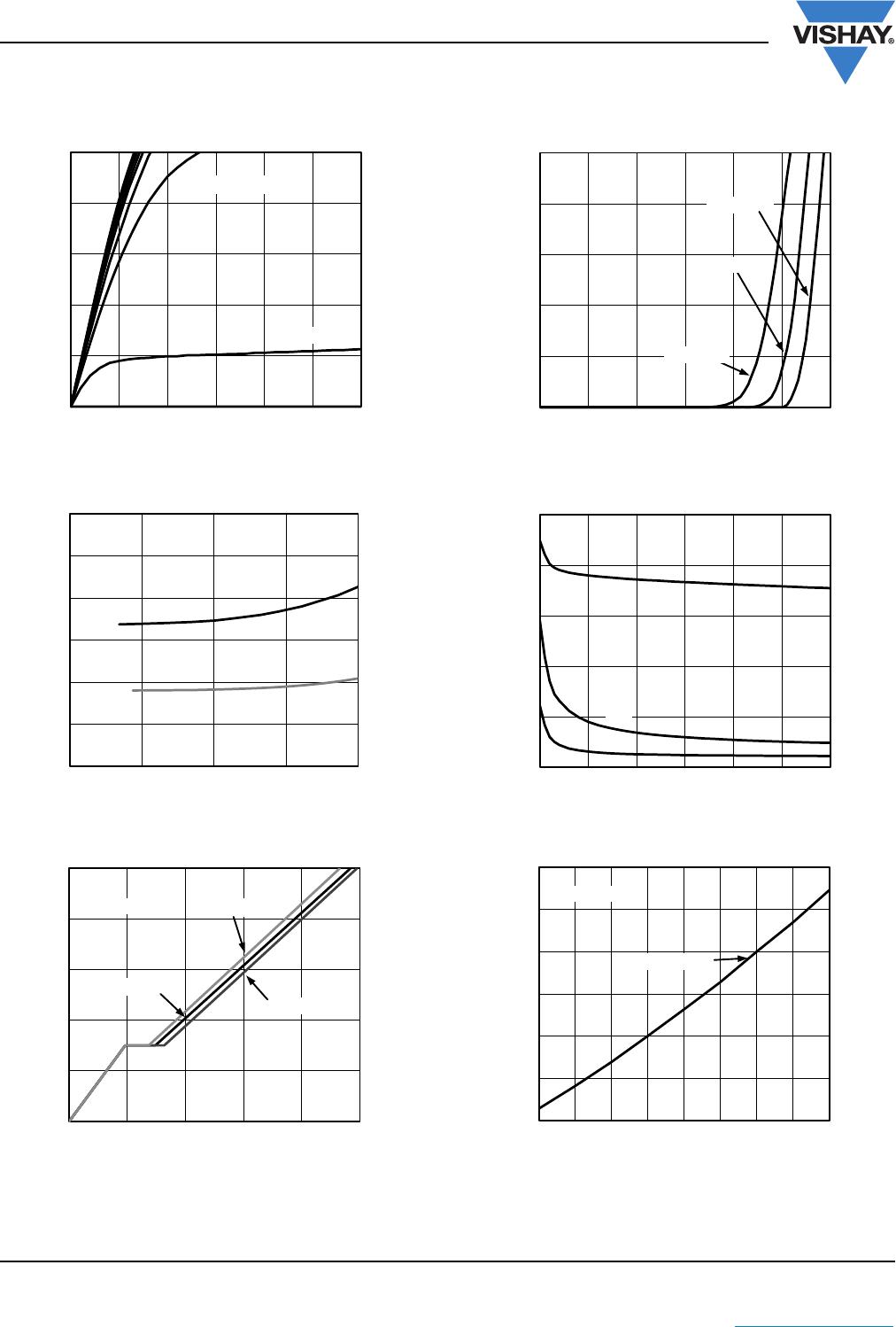
CHANNEL-1 TYPICAL CHARACTERISTICS (25 °C, unless otherwise noted)
Output Characteristics
On-Resistance vs. Drain Current
Gate Charge
0
20
40
60
80
100
0.0 0.5 1.0 1.5 2.0 2.5 3.0
I
D
- Drain Current (A)
V
DS
- Drain-to-Source Voltage (V)
V
GS
= 10 V thru 4 V
V
GS
= 3 V
0.004
0.005
0.006
0.007
0.008
0.009
0.010
0 20 40 60 80
R
DS(on)
- On-Resistance (Ω)
I
D
- Drain Current (A)
V
GS
= 4.5 V
V
GS
= 10 V
0
2
4
6
8
10
0 6 12 18 24 30
V
GS
- Gate-to-Source Voltage (V)
Q
g
- Total Gate Charge (nC)
V
DS
= 24 V
V
DS
= 15 V
V
DS
= 7.5 V
I
D
= 18.8 A
Transfer Characteristics
Capacitance
On-Resistance vs. Junction Temperature
0
4
8
12
16
20
0.0 0.5 1.0 1.5 2.0 2.5 3.0
I
D
- Drain Current (A)
V
GS
- Gate-to-Source Voltage (V)
T
C
= - 55 °C
T
C
= 25 °C
T= 125 °C
C
0
500
1000
1500
2000
2500
0 5 10 15 20 25 30
C - Capacitance (pF)
V
DS
- Drain-to-Source Voltage (V)
C
iss
C
oss
C
rss
0.6
0.8
1.0
1.2
1.4
1.6
1.8
- 50 - 25 0 25 50 75 100 125 150
R
DS(on)
- On-Resistance (Normalized)
T
J
- Junction Temperature (°C)
I
D
= 19.4 A
V
GS
= 10 V, 4.5 V