AD7910/AD7920
Rev. C | Page 7 of 24
TIMING EXAMPLES
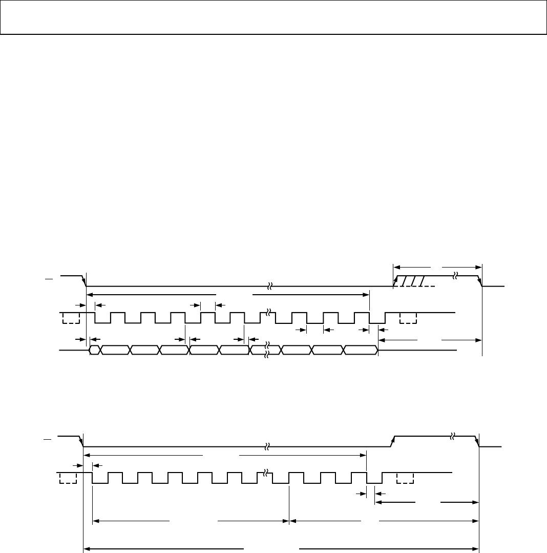
Figure 3 and Figure 4 show some of the timing parameters from
Table 3.
TIMING EXAMPLE 1
From Figure 4, having f
SCLK
= 5 MHz and a throughput rate of
250 kSPS gives a cycle time of t
2
+ 12.5(1/f
SCLK
) + t
ACQ
= 4 μs.
With t
2
= 10 ns min, this leaves t
ACQ
to be 1.49 μs. This 1.49 μs
satisfies the requirement of 250 ns for t
ACQ
. From Figure 4, t
ACQ
comprises 2.5(1/f
SCLK
) + t
8
+ t
QUIET
, where t
8
= 36 ns max. This
allows a value of 954 ns for t
QUIET
, satisfying the minimum
requirement of 50 ns.
TIMING EXAMPLE 2
The AD7920 can also operate with slower clock frequencies.
From
Figure 4, having f
SCLK
= 3.4 MHz and a throughput rate of
150 kSPS gives a cycle time of t
2
+ 12.5(1/f
SCLK
) + t
ACQ
= 6.66 μs.
With t
2
= 10 ns min, this leaves t
ACQ
to be 2.97 μs. This 2.97 μs
satisfies the requirement of 250 ns for t
ACQ
. From Figure 4, t
ACQ
comprises 2.5(1/f
SCLK
) + t
8
+ t
QUIET
, t
8
= 36 ns max. This allows a
value of 2.19 μs for t
QUIET
, satisfying the minimum requirement
of 50 ns. As in this example and with other slower clock values,
the signal may already be acquired before the conversion is
complete, but it is still necessary to leave 50 ns minimum t
QUIET
between conversions. In this example, the signal should be fully
acquired at approximately Point C in
Figure 4.
CS
SCLK
SDATA
t
2
t
6
t
3
t
4
t
7
t
5
t
8
t
CONVERT
t
QUIET
ZERO ZERO ZERO DB11 DB10 DB2 DB1 DB0
B
THREE-STATETHREE-
STATE
Z
4 LEADING ZEROS
12345 13141516
t
1
02976-003
Figure 3. AD7920 Serial Interface Timing Diagram
CS
S
CLK
t
2
t
CONVERT
B
12345 13141516
C
t
8
t
QUIET
t
ACQ
12.5(1/f
SCLK
)
1/THROUGHPUT
02976-004
Figure 4. Serial Interface Timing Example
AD7910/AD7920
Rev. C | Page 8 of 24
ABSOLUTE MAXIMUM RATINGS
T
A
= 25°C, unless otherwise noted.
Table 4.
Parameter Rating
V
DD
to GND −0.3 V to +7 V
Analog Input Voltage to GND −0.3 V to V
DD
+ 0.3 V
Digital Input Voltage to GND −0.3 V to +7 V
Digital Output Voltage to GND −0.3 V to V
DD
+ 0.3 V
Input Current to Any Pin Except Supplies
1
± 10 mA
Operating Temperature Range
Commercial (A, B Grade) −40°C to +85°C
Storage Temperature Range −65°C to +150°C
Junction Temperature 150°C
MSOP Package
θ
JA
Thermal Impedance 205.9°C/W
θ
JC
Thermal Impedance 43.74°C/W
SC70 Package
θ
JA
Thermal Impedance 340.2°C/W
θ
JC
Thermal Impedance 228.9°C/W
Lead Temperature, Soldering
Reflow (10 sec to 30 sec) 235 (0/+5)°C
ESD 3.5 kV
1
Transient currents of up to 100 mA will not cause SCR latch-up.
Stresses above those listed under Absolute Maximum Ratings
may cause permanent damage to the device. This is a stress
rating only; functional operation of the device at these or any
other conditions above those indicated in the operational
section of this specification is not implied. Exposure to absolute
maximum rating conditions for extended periods may affect
device reliability.
ESD CAUTION
ESD (electrostatic discharge) sensitive device. Electrostatic charges as high as 4000 V readily accumulate on
the human body and test equipment and can discharge without detection. Although this product features
proprietary ESD protection circuitry, permanent damage may occur on devices subjected to high energy
electrostatic discharges. Therefore, proper ESD precautions are recommended to avoid performance
degradation or loss of functionality.
AD7910/AD7920
Rev. C | Page 9 of 24
PIN CONFIGURATIONS AND FUNCTION DESCRIPTIONS
V
DD
1
GND
2
V
IN
3
CS
6
SDATA
5
SCLK
4
AD7910/
AD7920
TOP VIEW
(Not to Scale)
02976-005
Figure 5. 6-Lead SC70 Pin Configuration
V
DD
1
SDATA
2
CS
3
NC
4
V
IN
8
GND
7
SCLK
6
NC
5
NC = NO CONNECT
AD7910/
AD7920
TOP VIEW
(Not to Scale)
02976-006
Figure 6. 8-Lead MSOP Pin Configuration
Table 5. Pin Function Descriptions
Pin No.
6-Lead
SC70
Pin No.
8-Lead
MSOP
Mnemonic Description
6 3
CS Chip Select. Active low logic input. This input provides the dual function of initiating conversions on the
AD7910/AD7920 and framing the serial data transfer.
1 1 V
DD
Power Supply Input. The V
DD
range for the AD7910/AD7920 is from 2.35 V to 5.25 V.
2 7 GND
Analog Ground. Ground reference point for all circuitry on the AD7910/AD7920. All analog input signals
should be referred to this GND voltage.
3 8 V
IN
Analog Input. Single-ended analog input channel. The input range is 0 to V
DD
.
5 2 SDATA
Data Out. Logic output. The conversion result from the AD7910/AD7920 is provided on this output as a
serial data stream. The bits are clocked out on the falling edge of the SCLK input. The data stream from
the AD7920 consists of four leading zeros followed by the 12 bits of conversion data, which is provided
MSB first. The data stream from the AD7910 consists of four leading zeros followed by the 10 bits of
conversion data followed by two trailing zeros, which is also provided MSB first.
4 6 SCLK
Serial Clock. Logic input. SCLK provides the serial clock for accessing data from the part. This clock input
is also used as the clock source for the AD7910/AD7920 conversion process.
N/A 4, 5 NC No Connect.

AD7910ARMZ

Mfr. #:
Manufacturer:
Analog Devices Inc.
Description:
Analog to Digital Converters - ADC 250 kSPS 10-Bit IC
Lifecycle:
New from this manufacturer.
Delivery:
DHL FedEx Ups TNT EMS
Payment:
T/T Paypal Visa MoneyGram Western Union