General Description
The MAX6365–MAX6368 supervisory circuits simplify
power-supply monitoring, battery-backup control func-
tions, and memory write protection in microprocessor
(µP) systems. The circuits significantly improve the size,
accuracy, and reliability of modern systems with an ultra-
small integrated solution.
These devices perform four basic system functions:
1) Provide a µP reset output during V
CC
supply power-
up, power-down, and brownout conditions.
2) Internally control V
CC
to backup-battery switching to
maintain data or low-power operation for CMOS
RAM, CMOS µPs, real-time clocks, and other digital
logic when the main supply fails.
3) Provide memory write protection through internal
chip-enable gating during supply or processor faults.
4) Include one of the following options: a manual reset
input (MAX6365), a watchdog timer function
(MAX6366), a battery-on output (MAX6367), or an
auxiliary user-adjustable reset input (MAX6368).
The MAX6365–MAX6368 operate from V
CC
supply volt-
ages as low as 1.2V. The factory preset reset threshold
voltages range from 2.32V to 4.63V (see the
Ordering
Information
). In addition, each part is offered in three
reset output versions: push-pull active low, open-drain
active low, or open-drain active high (see the
Selector
Guide
). The MAX6365–MAX6368 are available in minia-
ture 8-pin SOT23 packages.
Applications
Critical µP/µC Power Portable/Battery-
Monitoring Powered Equipment
Fax Machines Set-Top Boxes
Industrial Control POS Equipment
Computers/Controllers
Features
o Low +1.2V Operating Supply Voltage (V
CC
or V
BATT
)
o Precision Monitoring of +5.0V, +3.3V, +3.0V, and
+2.5V Power-Supply Voltages
o On-Board Gating of Chip-Enable Signals, 1.5ns
Propagation Delay
o Debounced Manual Reset Input (MAX6365)
o Watchdog Timer, 1.6s Timeout (MAX6366)
o Battery-On Output Indicator (MAX6367)
o Auxiliary User-Adjustable RESET IN (MAX6368)
o Low 10µA Quiescent Supply Current
o Three Available Output Structures
Push-Pull RESET
Open-Drain RESET
Open-Drain RESET
o RESET/RESET Valid Down to 1.2V Guaranteed
(V
CC
or V
BATT
)
o Power-Supply Transient Immunity
o 150ms min Reset Timeout Period
o Miniature 8-Pin SOT23 Package
MAX6365–MAX6368
SOT23, Low-Power µP Supervisory Circuits
with Battery Backup and Chip-Enable Gating
________________________________________________________________
Maxim Integrated Products
1
OUT
V
CC
MR
1
2
8
7
CE OUT
BATTCE IN
GND
RESET, RESET
SOT23
TOP VIEW
3
4
6
5
MAX6365
Pin Configurations
19-1658; Rev 5; 10/11
For pricing, delivery, and ordering information, please contact Maxim Direct at 1-888-629-4642,
or visit Maxim’s website at www.maxim-ic.com.
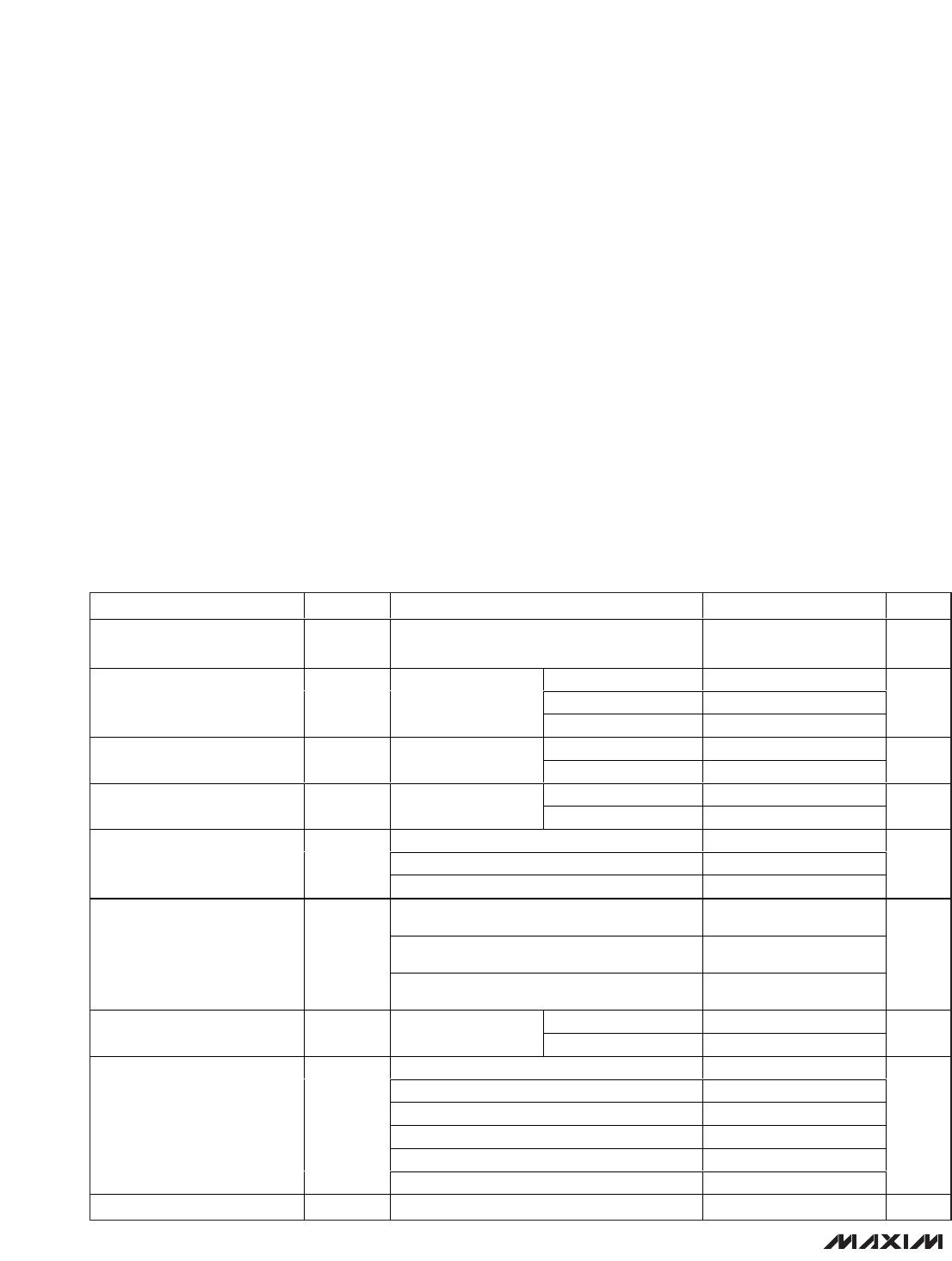
Ordering Information
*
These parts offer a choice of reset threshold voltages. From the
Reset Threshold Ranges table, insert the desired threshold volt-
age code in the blank to complete the part number. SOT parts
come in tape and reel only and must be ordered in 2500-piece
increments. See Device Marking Codes for a complete parts list,
including SOT top marks and standard threshold versions. See
Selector Guide for a listing of device features.
Devices are available in both leaded and lead(Pb)-free packaging.
Specify lead-free by replacing “-T” with “+T” when ordering.
-
Denotes a package containing lead(Pb).
T
= Tape and reel.
/V Denotes an automotive qualified part.
Pin Configurations continued at end of data sheet.
Typical Operating Circuit appears at end of data sheet.
PART*
TEMP RANGE
PIN-PACKAGE
M A X6 3 6 5 LK A_ _-T
-40°C to +85°C
8 SOT23
MAX6365PKA_ _-T
-40°C to +85°C
8 SOT23
MAX6365HKA_ _-T
-40°C to +85°C
8 SOT23
M A X6 3 6 6 LK A_ _-T
-40°C to +85°C
8 SOT23
M A X 6 36 6P K A_ _-T
-40°C to +85°C
8 SOT23
M A X 6 36 6H K A_ _-T
-40°C to +85°C
8 SOT23
M A X6 3 6 7 LK A_ _-T
-40°C to +85°C
8 SOT23
M A X 6 36 7P K A_ _-T
-40°C to +85°C
8 SOT23
M A X 6 36 7P K A_ _/V-T
-40°C to +85°C
8 SOT23
M A X 6 36 7H K A_ _-T
-40°C to +85°C
8 SOT23
M A X6 3 6 8 LK A_ _-T
-40°C to +85°C
8 SOT23
M A X 6 36 8P K A_ _-T
-40°C to +85°C
8 SOT23
M A X 6 36 8H K A_ _-T
-40°C to +85°C
8 SOT23
MAX6365–MAX6368
SOT23, Low-Power µP Supervisory Circuits
with Battery Backup and Chip-Enable Gating
2 _______________________________________________________________________________________
ABSOLUTE MAXIMUM RATINGS
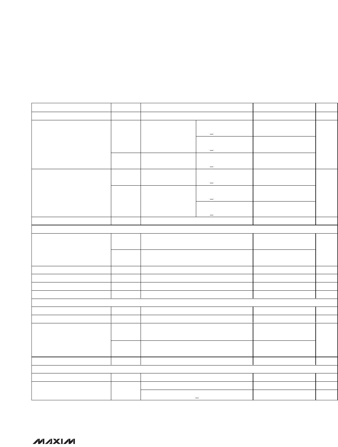
ELECTRICAL CHARACTERISTICS
(V
CC
= +2.4V to +5.5V, V
BATT
= +3.0V, CE IN = V
CC
, reset not asserted, T
A
= -40°C to +85°C. Typical values are at T
A
= +25°C,
unless otherwise noted.) (Note 1)
Stresses beyond those listed under “Absolute Maximum Ratings” may cause permanent damage to the device. These are stress ratings only, and functional
operation of the device at these or any other conditions beyond those indicated in the operational sections of the specifications is not implied. Exposure to
absolute maximum rating conditions for extended periods may affect device reliability.
Terminal Voltages (with respect to GND)
V
CC
, BATT, OUT.......................................................-0.3V to +6V
RESET (open drain), RESET (open drain) ................-0.3V to +6V
BATT ON, RESET (push-pull), RESET IN,
WDI, CE IN, CE OUT ...........................-0.3V to (V
OUT
+ 0.3V)
MR ..............................................................-0.3V to (V
CC
+ 0.3V)
Input Current
V
CC
Peak ..............................................................................1A
V
CC
Continuous .............................................................250mA
BATT Peak .....................................................................250mA
BATT Continuous .............................................................40mA
GND ...............................................................................75mA
Output Current
OUT ...............................Short-Circuit Protected for up to 10s
RESET, RESET, BATT ON, CE OUT...............................20mA
Continuous Power Dissipation (T
A
= +70°C)
8-Pin SOT23 (derate 8.75mW/°C above +70°C)........700mW
Operating Temperature Range ...........................-40°C to +85°C
Storage Temperature Range .............................-65°C to +150°C
Junction Temperature .....................................................+150°C
Lead Temperature (soldering, 10s) .................................+300°C
Soldering Temperature (reflow)
Lead (Pb)-free packages..............................................+260°C
Packages containing lead (Pb).....................................+240°C
PARAMETER
SYMBOL
CONDITIONS
MIN TYP MAX
UNITS
Operating Voltage Range
(Note 2)
V
CC
, V
BATT
No load 0 5.5 V
V
CC
= 2.8V 10 30
V
CC
= 3.6V 12 35
Supply Current
(Excluding I
OUT
)
I
CC
No load, V
CC
> V
TH
V
CC
= 5.5V 15 50
µA
T
A
= +25°C1
Supply Current in Battery-
Backup Mode (Excluding I
OUT
)
I
BACK
V
BATT
= 2.8V,
V
CC
= 0V
T
A
= -40°C to +85°C3
µA
T
A
= +25°C
-0.10 +0.02
BATT Standby Current I
BATT
5.5V > V
CC
> (V
BATT
+ 0.2V)
T
A
= -40°C to +85°C
-1.00 +0.05
µA
V
CC
= 4.75V, I
OUT
= 150mA 3.1
V
CC
= 3.15V, I
OUT
= 65mA 3.7V
CC
to OUT On-Resistance R
ON
V
CC
= 2.38V, I
OUT
= 25mA 4.6
V
BATT
= 4.5V, I
OUT
= 20mA
V
BATT
-
0.2
V
BATT
= 3.0V, I
OUT
= 10mA
V
BATT
-
0.15
Output Voltage in Battery-
Backup Mode
V
OUT
V
BATT
= 2.25V, I
OUT
= 5mA
V
BATT
-
0.15
V
Power-up 20
Battery-Switchover Threshold
(V
CC
- V
BATT
)
V
SW
V
CC
< V
TH
Power-down -20
mV
MAX636_ _KA46
4.50 4.63 4.75
MAX636_ _KA44
4.25 4.38 4.50
MAX636_ _KA31
3.00 3.08 3.15
MAX636_ _KA29
2.85 2.93 3.00
MAX636_ _KA26
2.55 2.63 2.70
Reset Threshold V
TH
MAX636_ _KA23
2.25 2.32 2.38
V
V
CC
Falling Reset Delay t
RD
V
CC
falling at 10V /ms 20 µs
MAX6365–MAX6368
SOT23, Low-Power µP Supervisory Circuits
with Battery Backup and Chip-Enable Gating
_______________________________________________________________________________________ 3
ELECTRICAL CHARACTERISTICS (continued)
(V
CC
= +2.4V to +5.5V, V
BATT
= +3.0V, CE IN = V
CC
, reset not asserted, T
A
= -40°C to +85°C. Typical values are at T
A
= +25°C,
unless otherwise noted.) (Note 1)
PARAMETER SYMBOL CONDITIONS MIN TYP MAX UNITS
Reset Active Timeout Period t
RP
150 280 ms
I
SINK
= 1.6mA,
V
CC
> 2.1V
0.3
V
OL
Reset asserted,
V
BATT
= 0V
I
SINK
= 100µA,
V
CC
> 1.2V
0.4
RESET Output Voltage
V
OH
Reset not asserted
(MAX636_L only)
I
SOURCE
= 500µA,
V
CC
> V
TH(MAX)
0.8
V
CC
V
V
OL
Reset not asserted
I
SINK
= 1.6mA,
V
CC
> V
TH (MAX)
0.3
I
SOURCE
= 1mA,
V
CC
> 1.8V
0.7
V
CC
RESET Output Voltage
V
OH
Reset not asserted,
V
BATT
= 0V
(MAX636_H only)
(Note 3)
I
SOURCE
= 200µA,
V
CC
> 1.2V
0.8
V
CC
V
RE S E T Outp ut Leakag e C ur r ent I
LKG
MAX636_P and MAX636_H only 1 µA
MANUAL RESET (MAX6365 only)
V
IL
0.3
V
CC
MR Input Voltage
V
IH
0.7
V
CC
V
Pullup Resistance 20 k
Minimum Pulse Width s
Glitch Immunity V
CC
= 3.3V 100 ns
MR to Reset Delay V
CC
= 3.3V 120 ns
WATCHDOG (MAX6366 only)
Watchdog Timeout Period t
WD
1.00 1.65 2.25 s
Minimum WDI Input Pulse Width t
WDI
100 ns
V
IL
0.3
V
CC
WDI Input Voltage
V
IH
0.7
V
CC
V
WDI Input Current -1.0 1.0 µA
BATT ON (MAX6367 only)
Output Voltage V
OL
I
SINK
= 3.2mA, V
BATT
= 2.1V 0.4 V
Sink current, V
CC
= 5V 60 mA
Output Short-Circuit Current
Source current, V
BATT
> 2V 10 30 100 µA

MAX6365LKA29+T

Mfr. #:
Manufacturer:
Maxim Integrated
Description:
Supervisory Circuits uPower Supervisor
Lifecycle:
New from this manufacturer.
Delivery:
DHL FedEx Ups TNT EMS
Payment:
T/T Paypal Visa MoneyGram Western Union