MAX6365–MAX6368
SOT23, Low-Power µP Supervisory Circuits
with Battery Backup and Chip-Enable Gating
_______________________________________________________________________________________ 7
Pin Description
PIN NAME FUNCTION
RESET
Acti ve- H i g h Reset Outp ut. RE S E T asser ts hi g h conti nuousl y w hen V
C C
i s b el ow the r eset thr eshol d ( V
TH
) ,
M R i s l ow , or RE S E T IN i s l ow . It asser ts i n p ul ses w hen the inter nal w atchd og ti m es out. RE S E T r em ai ns
asser ted for the r eset ti m eout p er i od ( t
RP
) after V
C C
r i ses ab ove the r eset thr eshol d , after the m anual r eset
i np ut g oes fr om l ow to hi g h, after RE S E T IN g oes hi g h, or after the w atchd og tr i g g ers a r eset event.
RE S E T i s an op en- d r ai n acti ve- hi g h r eset outp ut.
1
RESET
Active-Low Reset Output. RESET asserts low continuously when V
C C
is below the reset threshold
(V
TH
), the manual reset input is low, or RESET IN is low. It asserts low in pulses when the internal
watchdog times out. RESET remains asserted low for the reset timeout period (t
RP
) after V
C C
rises above the reset threshold, after the manual reset input goes from low to high, after RESET
IN goes high, or after the watchdog triggers a reset event. The MAX636_L is an active-low push-
pull output, while the MAX636_P is an active-low open-drain output.
2 CE IN
Chip-Enable Input. The input to chip-enable gating circuitry. Connect to GND or OUT if not used.
3 GND Ground
MR
MAX6365 Manual-Reset Input. Maintaining logic low on MR asserts a reset. Reset output
remains asserted as long as MR is low and for the reset timeout period (t
RP
) after MR transitions
from low to high. Leave unconnected, or connect to V
CC
if not used. MR has an internal 20k
pullup to V
CC
.
WDI
MAX6366 Watchdog Input. If WDI remains high or low for longer than the watchdog timeout
period (t
W D
), the internal watchdog timer runs out and a reset pulse is triggered for the reset
timeout period (t
RP
). The internal watchdog clears whenever reset asserts or whenever WDI sees
a rising or falling edge (Figure 2).
BATT ON MAX6367 Battery-On Output. BATT ON goes high when in battery-backup mode.
4
RESET IN
MAX6368 Reset Input. When RESET IN falls below 1.235V, reset asserts. Reset output remains
asserted as long as RESET IN is low and for at least t
RP
after RESET IN goes high.
5V
CC
Supply Voltage, 1.2V to 5.5V. Reset asserts when V
C C
drops below the reset threshold voltage
(V
TH
). Reset remains asserted until V
C C
rises above V
TH
and for at least t
RP
after V
C C
rises
above V
TH
.
6 OUT
Output. OUT sources from V
C C
when not in reset and from the greater of V
CC
or BATT when V
C C
is below the reset threshold.
7 BATT
Backup-Battery Input. When V
C C
falls below the reset threshold, OUT switches to BATT
if V
BATT
is 20mV greater than V
C C
. When V
C C
rises 20mV above V
BATT
, OUT switches to V
C C
. The 40mV
hysteresis prevents repeated switching if V
CC
falls slowly.
8 CE OUT
Chip-Enable Output. CE OUT goes low only when CE IN is low and reset is not asserted. If CE
IN is low when reset is asserted, CE OUT will stay low for 12µs (typ) or until CE IN goes high,
whichever occurs first.
MAX6365–MAX6368
SOT23, Low-Power µP Supervisory Circuits
with Battery Backup and Chip-Enable Gating
8 _______________________________________________________________________________________
MAX6365
MAX6366
MAX6367
MAX6368
CHIP-ENABLE
OUTPUT
CONTROL
V
CC
BATT
CE IN
20k
MR
(MAX6365 ONLY)
WDI
(MAX6366 ONLY)
RESET IN
(MAX6368 ONLY)
RESET
GENERATOR
WATCHDOG
TRANSITION
DETECTOR
WATCHDOG
TIMER
1.235V
GND
1.235V
RESET
(RESET)
CE OUT
OUT
BATT ON (MAX6367 ONLY)
Detailed Description
The
Typical Operating Circuit
shows a typical connec-
tion for the MAX6365–MAX6368. OUT powers the static
random-access memory (SRAM). If V
CC
is greater than
the reset threshold (V
TH
), or if V
CC
is lower than V
TH
but higher than V
BATT
, V
CC
is connected to OUT. If
V
CC
is lower than V
TH
and V
CC
is less than V
BATT
,
BATT is connected to OUT. OUT supplies up to 150mA
from V
CC
. In battery-backup mode, an internal MOSFET
connects the backup battery to OUT. The on-resistance
of the MOSFET is a function of backup-battery voltage
and is shown in the BATT-to-OUT On-Resistance vs.
Temperature graph in the
Typical Operating Char-
acteristics
.
Chip-Enable Signal Gating
The MAX6365–MAX6368 provide internal gating of CE
signals to prevent erroneous data from being written to
CMOS RAM in the event of a power failure. During nor-
mal operation, the CE gate is enabled and passes all
CE transitions. When reset asserts, this path becomes
disabled, preventing erroneous data from corrupting
the CMOS RAM. All of these devices use a series trans-
mission gate from CE IN to CE OUT. The 2ns propaga-
tion delay from CE IN to CE OUT allows the devices to
be used with most µPs and high-speed DSPs.
During normal operation, CE IN is connected to CE
OUT through a low on-resistance transmission gate.
This is valid when reset is not asserted. If CE IN is high
when reset is asserted, CE OUT remains high regard-
less of any subsequent transitions on CE IN during the
reset event.
If CE IN is low when reset is asserted, CE OUT is held
low for 12µs to allow completion of the read/write oper-
ation (Figure 1). After the 12µs delay expires, the CE
Functional Diagram
MAX6365–MAX6368
SOT23, Low-Power µP Supervisory Circuits
with Battery Backup and Chip-Enable Gating
_______________________________________________________________________________________ 9
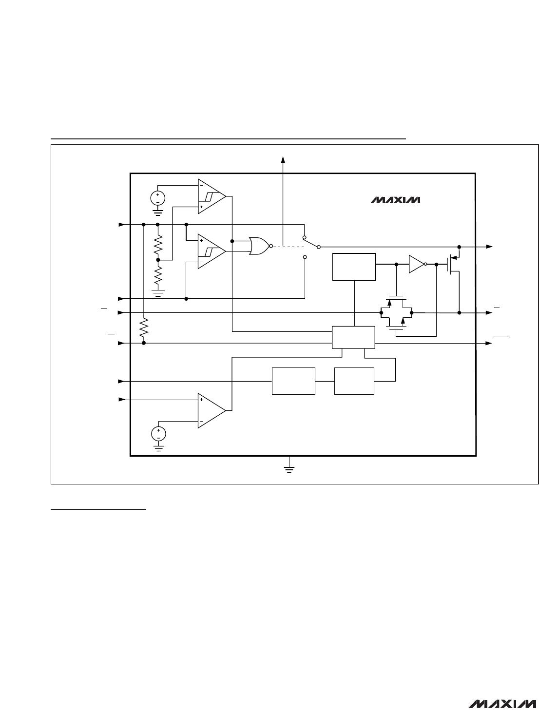
OUT goes high and stays high regardless of any sub-
sequent transitions on CE IN during the reset event.
When CE OUT is disconnected from CE IN, CE OUT is
actively pulled up to OUT.
The propagation delay through the chip-enable circuit-
ry depends on both the source impedance of the drive
to CE IN and the capacitive loading at CE OUT. The
chip-enable propagation delay is production tested
from the 50% point of CE IN to the 50% point of CE
OUT, using a 50 driver and 50pF load capacitance.
Minimize the capacitive load at CE OUT to minimize
propagation delay, and use a low-output-impedance
driver.
Backup-Battery Switchover
In a brownout or power failure, it may be necessary to
preserve the contents of the RAM. With a backup bat-
tery installed at BATT, the MAX6365–MAX6368 auto-
matically switch the RAM to backup power when V
CC
falls. The MAX6367 has a BATT ON output that goes
high in battery-backup mode. These devices require
two conditions before switching to battery-backup
mode:
1) V
CC
must be below the reset threshold.
2) V
CC
must be below V
BATT
.
Table 1 lists the status of the inputs and outputs in bat-
tery-backup mode. The devices do not power up if the
only voltage source is on BATT. OUT only powers up
from V
CC
at startup.
Manual Reset Input (MAX6365 Only)
Many µP-based products require manual reset capabili-
ty, allowing the user or external logic circuitry to initiate a
reset. For the MAX6365, a logic low on MR asserts reset.
Reset remains asserted while MR is low and for a mini-
mum of 150ms (t
RP
) after it returns high. MR has an inter-
nal 20k pullup resistor to V
CC
. This input can be driven
with TTL/CMOS logic levels or with open-drain/collector
outputs. Connect a normally open momentary switch
from MR to GND to create a manual reset function; exter-
nal debounce circuitry is not required. If MR is driven
from long cables or the device is used in a noisy environ-
ment, connect a 0.1µF capacitor from MR to GND to pro-
vide additional noise immunity.
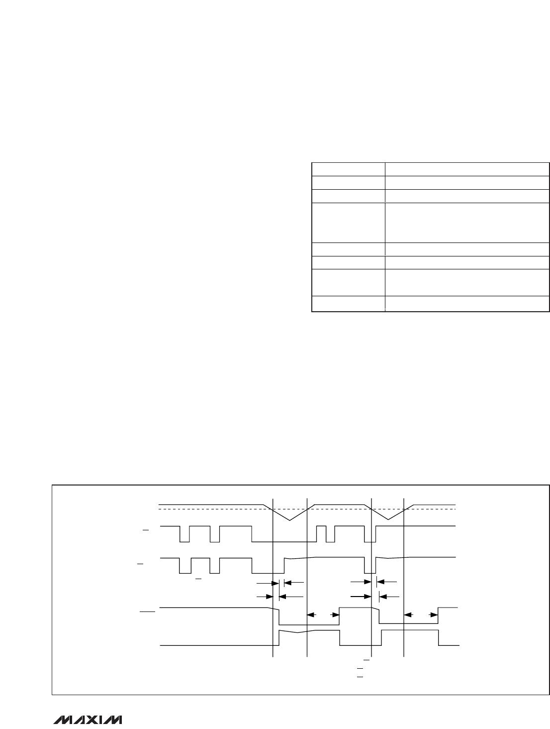
Figure 1. Reset and Chip-Enable Timing
V
CC
OR BATT
RESET
THRESHOLD V
TH
RESET
CE IN
CE OUT
RESET
*
t
RD
t
RD
t
RP
t
RP
IF CE IN GOES HIGH BEFORE RESET ASSERTS,
CE OUT GOES HIGH WITHOUT DELAY AS
CE IN GOES HIGH.
RESET-TO-CE OUT DELAY (12µs)
*
PIN STATUS
V
CC
Disconnected from OUT
OUT Connected to BATT
BATT
Connected to OUT. Current drawn from
the battery is less than 1µA (at V
BATT
=
2.8V, excluding I
OUT
) when V
CC
= 0V.
RESET/RESET Asserted
BATT ON High state
MR, RESET IN,
CE IN, WDI
Inputs ignored
CE OUT Connected to OUT
Table 1. Input and Output Status in
Battery-Backup Mode

MAX6365LKA29+T

Mfr. #:
Manufacturer:
Maxim Integrated
Description:
Supervisory Circuits uPower Supervisor
Lifecycle:
New from this manufacturer.
Delivery:
DHL FedEx Ups TNT EMS
Payment:
T/T Paypal Visa MoneyGram Western Union