ISL36111DRZ-T7

1
CAUTION: These devices are sensitive to electrostatic discharge; follow proper IC Handling Procedures.
1-888-INTERSIL or 1-888-468-3774
|Copyright Intersil Americas Inc. 2009, 2010, 2012. All Rights Reserved
Intersil (and design) is a trademark owned by Intersil Corporation or one of its subsidiaries.
All other trademarks mentioned are the property of their respective owners.
11.1Gb/s Lane Extender
ISL36111
The ISL36111 is a settable single-channel receive-side
equalizer with extended functionality for advanced protocols
operating with line rates up to 11.1Gb/s, such as 10G
Ethernet. The ISL36111 compensates for the frequency
dependent attenuation of copper twin-axial cables, extending
the signal reach up to at least 10m on 28AWG cable.
The small form factor, highly-integrated design is ideal for
high-density data transmission applications including active
copper cable assemblies. The equalizing filter within the
ISL36111 can be set to provide optimal signal fidelity for a
given media and length. The compensation level for the filter is
set by two external control pins.
Operating on a single 1.2V power supply, the ISL36111
enables channel throughputs of 10Gb/s to 11.1Gb/s while
supporting lower data rates including 8.5, 6.25, 5, 4.25, 3.125,
2.5 and 1 Gb/s. The ISL36111 uses current mode logic (CML)
input/output and is packaged in a 3mmx3mm
16 lead QFN.
The device supports LOS functionality for module applications.
Features
Supports data rates up to 11.1Gb/s
Low power (~110mW)
Low latency (<500ps)
Single channel equalizer in a 3mmx3mm QFN package for
straight route-through architecture and simplified routing
Adjustable equalizer boost
Supports 64b/66b encoded data – long run lengths
Line silence preservation
1.2V supply voltage
Loss of Signal support
Applications
SFP+ active copper cable modules
QSFP active copper cable modules
•10G Ethernet
•Fibre Channel
•High-speed active cable assemblies
High-speed printed circuit board (PCB) traces
Benefits
•Thinner gauge cable
Extends cable reach greater than 3x
•Improved BER
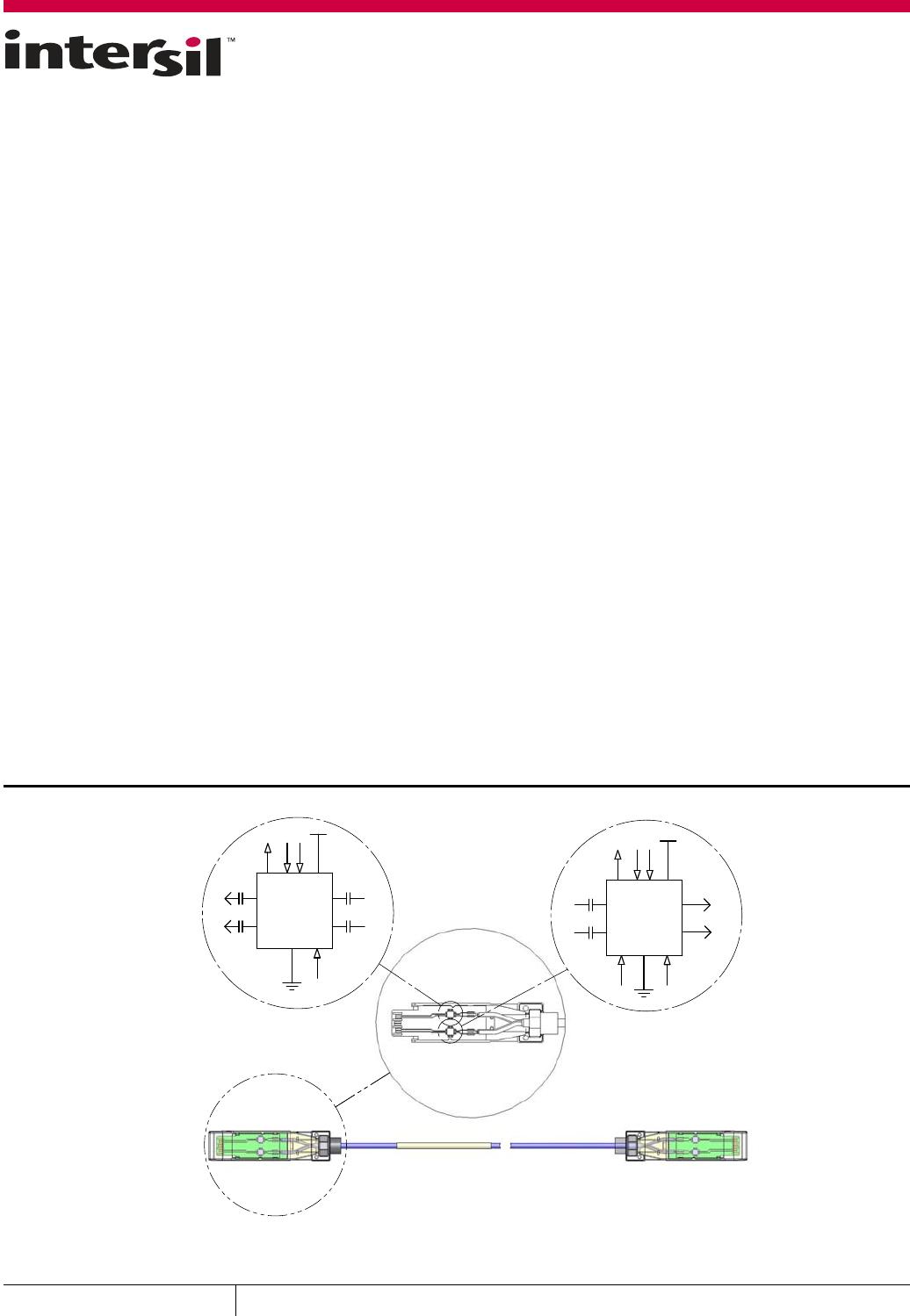
FIGURE 1. TYPICAL CABLE APPLICATION DIAGRAM
QLx111VRx
1.2V
LOS
CP-A
Vdd
0.1mF
IN [P]
OUT [P]
DT
CP-B
IN [N]
OUT [N]
0.1mF
0.1mF
IN [N]
Vdd
OUT [N]
OUT [P]
IN [P]
DT
LOS
DE-B
0.1mF
QLx111VTx
DE-A
1.2V
0.1mF
0.1mF
TDSBL
GND
GND
ISL35111
ISL36111
July 19, 2012
FN6974.2
ISL36111
2
FN6974.2
July 19, 2012
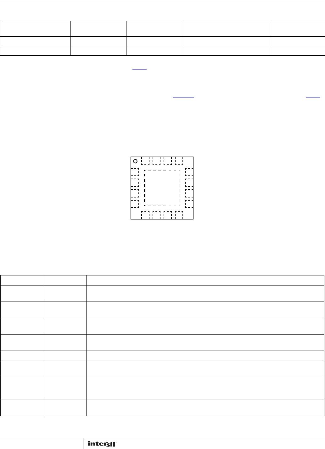
Pin Configuration
ISL36111
(16 LD QFN)
TOP VIEW
Ordering Information
PART NUMBER
(Notes 1, 2, 3)
PART
MARKING
TEMP. RANGE
(°C)
PACKAGE
(Pb-Free)
PKG.
DWG. #
ISL36111DRZ-TS 6111 0 to +85 16 Ld QFN (7’’ 100 pcs.) L16.3x3B
ISL36111DRZ-T7 6111 0 to +85 16 Ld QFN (7” 1k pcs.) L16.3x3B
NOTES:
1. “-TS” and “-T7” suffix is for Tape and Reel. Please refer to TB347
for details on reel specifications.
2. These Intersil Pb-free plastic packaged products employ special Pb-free material sets, molding compounds/die attach materials, and 100% matte
tin plate plus anneal (e3 termination finish, which is RoHS compliant and compatible with both SnPb and Pb-free soldering operations). Intersil
Pb-free products are MSL classified at Pb-free peak reflow temperatures that meet or exceed the Pb-free requirements of IPC/JEDEC J STD-020.
3. For Moisture Sensitivity Level (MSL), please see device information page for ISL36111
. For more information on MSL please see techbrief TB363.
1
3
4
15
V
DD
IN[P]
IN[N]
LOSB
GND
DT
NC
GND
16 14 13
2
12
10
9
11
6578
V
DD
OUT[P]
OUT[N]
V
DD
GND
CPA
CPB
GND
Pin Descriptions
PIN NAME PIN NUMBER DESCRIPTION
V
DD
1, 9, 12 Power supply. 1.2V supply voltage. The use of parallel 100pF and 47nF decoupling capacitors to ground is
recommended for each of these pins for broad high-frequency noise suppression.
IN[P,N] 2, 3 Equalizer differential input, CML. The use of 100nF low ESL/ESR MLCC capacitor with at least 6GHz frequency
response is recommended.
LOSB 4 LOS BAR indicator. Low output when input signal is below DT threshold. This pin is internally pulled HIGH with
an 11kΩ resistor.
CP[A,B] 6, 7 Control pins for setting equalizer boost level. Tri-state inputs. Pins are read as a 2-digit number to set the boost
level. A is the MSB, and B is the LSB.
GND 5, 8, 13, 16 These pins must be grounded.
OUT[P,N] 11, 10 Equalizer differential output, CML. The use of 100nF low ESL/ESR MLCC capacitor with at least 6GHz frequency
response is recommended.
DT 15 Detection Threshold. Reference DC voltage threshold for input signal power detection. Data output OUT[P,N] is
muted when the power of the input signal IN[P,N] falls below the threshold. Tie to ground to disable electrical idle
preservation and always enable the output driver.
Exposed Pad - Exposed pad. For proper electrical and thermal performance, this pad should be connected to the PCB ground
plane.
ISL36111
3
FN6974.2
July 19, 2012
Absolute Maximum Ratings Thermal Information
Supply Voltage (V
DD
to GND). . . . . . . . . . . . . . . . . . . . . . . . . . . -0.3V to 1.5V
Voltage at All Input Pins. . . . . . . . . . . . . . . . . . . . . . . . . . . . . . . -0.3V to 1.5V
ESD Rating
High-Speed Pins . . . . . . . . . . . . . . . . . . . . . . . . . . . . . . . . . . . .1.5kV (HBM)
All Other Pins . . . . . . . . . . . . . . . . . . . . . . . . . . . . . . . . . . . . . . . 2kV (HBM)
Thermal Resistance (Typical) θ
JA
(°C/W) θ
JC
(°C/W)
16 Ld QFN Package (Notes 4, 5) . . . . . . . . 56 10
Operating Ambient Temperature Range . . . . . . . . . . . . . . . . 0°C to +85°C
Storage Ambient Temperature Range . . . . . . . . . . . . . . . .-55°C to +150°C
Maximum Junction Temperature . . . . . . . . . . . . . . . . . . . . . . . . . . . .+125°C
Pb-Free Reflow Profile . . . . . . . . . . . . . . . . . . . . . . . . . . . . . . . see link below
http://www.intersil.com/pbfree/Pb-FreeReflow.asp
CAUTION: Do not operate at or near the maximum ratings listed for extended periods of time. Exposure to such conditions may adversely impact product
reliability and result in failures not covered by warranty.
NOTE:
4. θ
JA
measured in free air with the component mounted on a high effective thermal conductivity test board with “direct attach” features. See Tech Brief
TB379
.
5. For θ
JC
, the “case temp” location is the center of the exposed metal pad on the package underside.
Operating Conditions
PARAMETER SYMBOL CONDITION MIN TYP MAX UNITS
Supply Voltage V
DD
1.1 1.2 1.3 V
Operating Ambient Temperature T
A
02585°C
Bit Rate NRZ data applied to any channel 1 11.1 Gb/s
Control Pin Characteristics V
DD
= 1.2V, T
A
= +25°C, and V
IN
= 600mV
P-P
, unless otherwise noted.
PARAMETER SYMBOL CONDITION
MIN
(Note 14) TYP
MAX
(Note 14) UNITS
Output LOW Logic Level V
OL
LOSB 0 0 250 mV
Output HIGH Logic Level V
OH
LOSB 1000 V
DD
mV
Input Current Current draw on boost control pin, i.e., CP[A,B] 30 100 µA
Electrical Specifications V
DD
= 1.2V, T
A
= +25°C, and V
IN
= 600mV
P-P
, unless otherwise noted.
PARAMETERS SYMBOL CONDITION
MIN
(Note 14) TYP
MAX
(Note 14) UNITS NOTES
Supply Current I
DD
92 mA
Cable Input Amplitude Range V
IN
Measured differentially at data source before
encountering channel loss; Up to 10m 28AWG
standard twin-axial cable (approx. -27dB @ 5GHz)
600 1600 mV
P-P
6
DC Differential Input Resistance Measured on input channel IN[P,N] 80 100 120 Ω
DC Single-Ended Input Resistance Measured on input channel IN[P] or IN[N], with
respect to V
DD
.
40 50 60 Ω
Input Return Loss Limit
(Differential)
S
DD
11 100MHz to 4.1GHz Note 7 dB 7
4.1GHz to 11.1GHz Note 8 dB 8
Output Amplitude Range V
OUT
Measured differentially at OUT[P] and OUT[N]
with 50Ω load on both output pins
450 650 850 mV
P-P
Differential Output Impedance Measured on OUT[P,N] 80 105 120 Ω
Output Return Loss Limit
(Differential)
S
DD
22 100MHz to 4.1GHz Note 7 dB 7
4.1GHz to 11.1GHz Note 8 dB 8
Output Return Loss Limit (Common
Mode)
S
CC
22 100MHz to 2.5GHz Note 9 dB 9
2.5GHz to 11.1GHz -3 dB 10
ISL36111DRZ-T7

Mfr. #:
Manufacturer:
Renesas / Intersil
Description:
Equalizers ISL36111DRZ-EVALZ EVAL BRD RHS COMPLIA
Lifecycle:
New from this manufacturer.
Delivery:
DHL FedEx Ups TNT EMS
Payment:
T/T Paypal Visa MoneyGram Western Union

Products related to this Datasheet