ISL36111
5
FN6974.2
July 19, 2012
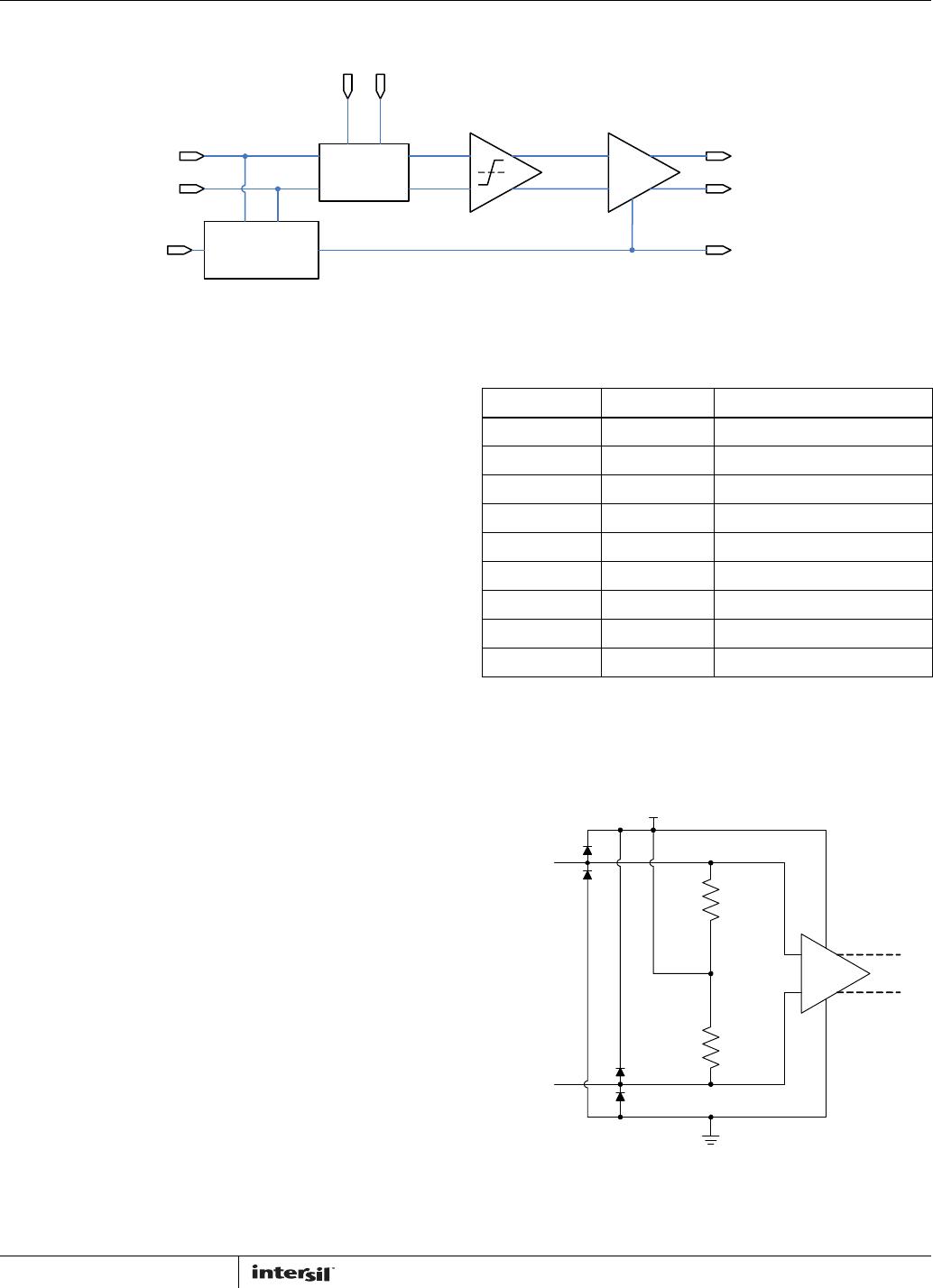
Operation
The ISL36111 is an advanced lane-extender for high-speed
interconnects. A functional diagram of ISL36111 is shown in
Figure 4. In addition to a robust equalization filter to compensate
for channel loss and restore signal fidelity, the ISL36111
contains unique integrated features to preserve special signaling
protocols typically broken by other equalizers. The signal detect
function is used to mute the channel output when the input
signal falls below the level determined by the Detection
Threshold (DT) pin voltage. This function is intended to preserve
periods of line silence (“DC idle”). Furthermore, the output of the
Signal Detect/DT comparator is used as a loss of signal (LOSB)
indicator to indicate the absence of a received signal.
As illustrated in Figure 4, the core of the high-speed signal path
in the ISL36111 is a sophisticated equalizer followed by a
limiting amplifier. The equalizer compensates for skin loss,
dielectric loss, and impedance discontinuities in the
transmission channel. The equalizer is followed by a limiting
amplification stage that provides a clean output signal with full
amplitude swing and fast rise-fall times for reliable signal
decoding in a subsequent receiver.
Adjustable Equalization Boost
ISL36111 features a settable equalizer for custom signal
restoration. The flexibility of this adjustable compensation
architecture enables signal fidelity to be optimized based on a
given application, providing support for a wide variety of channel
characteristics and data rates ranging from 2.5Gb/s to
11.1Gb/s. Because the boost level is externally set rather than
internally adapted, the ISL36111 provides reliable
communication from the very first bit transmitted. There is no
time needed for adaptation and control loop convergence.
Furthermore, there are no pathological data patterns that will
cause the ISL36111 to move to an incorrect boost level.
Control Pin Boost Setting
The connectivity of the CP pins are used to determine the boost
level of ISL36111. Table 1 defines the mapping from the 2-bit CP
word to the 9 available boost levels.
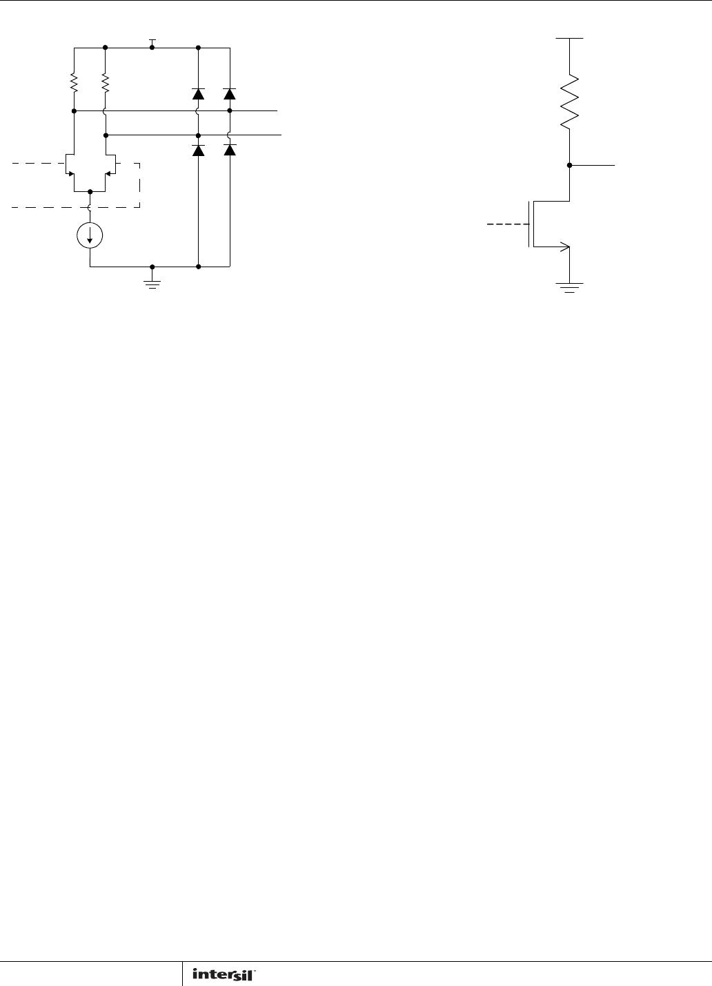
CML Input and Output Buffers
The input and output buffers for the high-speed data channel in
the ISL36111 are implemented using CML. Equivalent input and
output circuits are shown in Figures 5 and 6.
Signal
Detector
IN[P]
IN[N]
DT LOSB
OUT[N]
OUT[P]
Adjustable
Equalizer
CPA
CPB
Limiting
Amplifier
Output
Driver
FIGURE 4. FUNCTIONAL BLOCK DIAGRAM OF THE ISL36111
TABLE 1. MAPPING BETWEEN BOOST LEVEL AND CP-PIN
CONNECTIVITY
CPA CPB BOOST LEVEL
Float Float 0
Float GND 1
GND VDD 2
Float VDD 3
VDD Float 4
GND Float 5
GND GND 6
VDD GND 7
VDD VDD 8
IN[P]
IN[N]
1
st
Filter
Stage
V
DD
50O
50O
FIGURE 5. CML INPUT EQUIVALENT CIRCUIT FOR THE ISL36111
Ω
Ω