1
LT1803/LT1804/LT1805
180345f
FEATURES
DESCRIPTIO
U
APPLICATIO S
U
TYPICAL APPLICATIO
U
Single/Dual/Quad 100V/µs,
85MHz, Rail-to-Rail Input and
Output Op Amps
■
Slew Rate: 100V/µs
■
Gain Bandwidth Product: 85MHz
■
Input Common Mode Range Includes Both Rails
■
Output Swings Rail-to-Rail
■
Low Quiescent Current: 3mA Max per Amplifier
■
Large Output Current: 42mA
■
Voltage Noise: 21nV/√Hz
■
Power Supply Rejection: 90dB
■
Open-Loop Gain: 60V/mV
■
Operating Temperature Range: –40°C to 85°C
■
Single Available in the 8-Pin SO and 5-Pin Low Profile
(1mm) SOT-23 (ThinSOT
TM
) Package
■
Dual Available in 8-Lead DFN and SO Packages
■
Quad Available in the 14-Pin Narrow SO Package
■
Low Voltage, High Frequency Signal Processing
■
Driving A/D Converters
■
Rail-to-Rail Buffer Amplifiers
■
Active Filters
■
Video Line Driver
The LT
®
1803/LT1804/LT1805 are single/dual/quad, low
power, high speed rail-to-rail input and output operational
amplifiers with excellent DC performance. The LT1803/
LT1804/LT1805 feature reduced supply current, lower
input offset voltage, lower input bias current and higher
DC gain than other devices with comparable bandwidth
and slew rate.
Typically, the LT1803/LT1804/LT1805 have an input off-
set voltage of 350µV, an input bias current of 125nA and
an open-loop gain of 60V/mV.
The LT1803/LT1804/LT1805 have an input range that
includes both supply rails and an output that swings within
20mV of either supply rail to maximize the signal dynamic
range in low supply applications.
The LT1803/LT1804/LT1805 are specified at 3V, 5V and
±5V supplies and typically maintain their performance for
supplies from 2.3V to 12.6V. The inputs can be driven
beyond the supplies without damage or phase reversal of
the output.
The LT1803 is available in the 8-pin SO package with the
standard op amp pinout and in the 5-pin SOT-23 package.
The LT1804 is available in 8-pin DFN and SO packages
with the standard op amp pinouts. The LT1805 features
the standard quad op amp configuration and is available in
a 14-pin plastic SO package.
, LTC and LT are registered trademarks of Linear Technology Corporation.
–
+
–
+
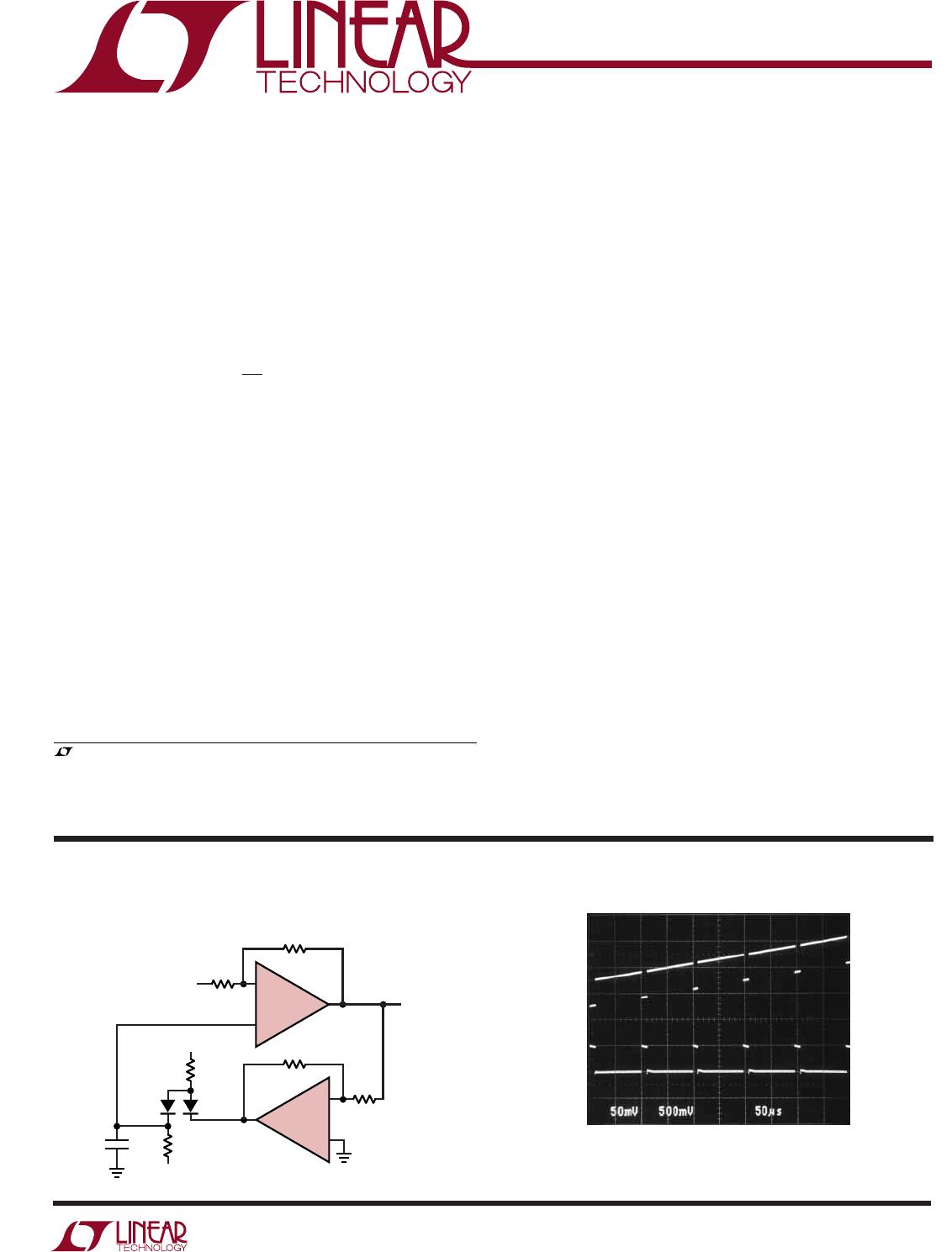
A
1/2 LT1804
B
1/2 LT1804
R2
10k
R4
100k
R5
2k
D1
1N4148
V
S
= ±5V
18045 TA01
D2
1N4148
R3
1k
R1
1k
V
IN
V
S
+
V
S
–
V
OUT
R6
1M
C1
0.1µF
Inverting DC Restore
50µs/DIV 18045 TA02
V
IN
50mV/DIV
GND
V
OUT
500mV/DIV
GND
Inverting DC Restore Circuit Response
ThinSOT is a trademark of Linear Technology Corporation.