13
LT1803/LT1804/LT1805
180345f
APPLICATIO S I FOR ATIO
WUUU
TYPICAL PERFOR A CE CHARACTERISTICS
UW
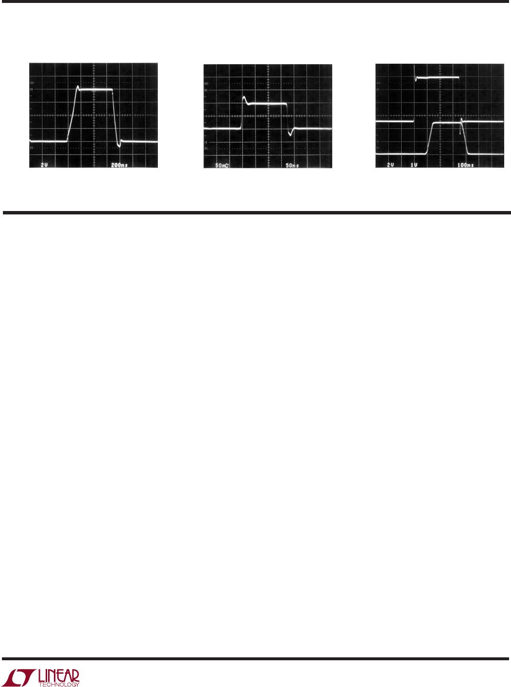
Output Overdrive Recovery
Circuit Description
The LT1803/LT1804/LT1805 have input and output signal
ranges from the negative power supply to the positive
power supply. Figure 1 depicts a simplified schematic of
one amplifier. The input stage is comprised of two differ-
ential amplifiers, a PNP stage Q1/Q2 and an NPN stage Q3/
Q4 that are active over the different ranges of the common
mode input voltage. The PNP differential pair is active
between the negative supply and approximately 1.3V
below the positive supply. As the input voltage moves
toward the positive supply, the transistor Q5 will steer the
tail current I
1
to the current mirror Q6/Q7 activating the
NPN differential pair. The PNP pair becomes inactive for
the rest of the input common mode range up to the positive
supply. Also at the input stage, devices Q18 and Q19 act
to cancel the bias current of the PNP input pair. When Q1
and Q2 are active, the current in Q16 is controlled to be the
same as the current in Q1 and Q2; therefore, the base
current of Q16 is nominally equal to the base current of the
input devices. The base current of Q16 is then mirrored by
devices Q17 through Q19 to cancel the base current of the
input devices Q1 and Q2.
A pair of complementary common emitter stages Q14/
Q15 that enable the output to swing from rail-to-rail
constructs the output stage. The capacitors C1 and C2
form the local feedback loops that lower the output
impedance at high frequency. The LT1803/LT1804/LT1805
are fabricated on Linear Technology’s proprietary high
speed complementary bipolar process.
Power Dissipation
There is a need to ensure that the die’s junction tempera-
ture does not exceed 150°C. Junction temperature T
J
is
calculated from the ambient temperature T
A
, power dissi-
pation P
D
and thermal resistance θ
JA
:
T
J
= T
A
+ (P
D
θ
JA
)
The power dissipated in the IC is a function of the supply
voltage, amplifier current, output voltage and output cur-
rent. For a given supply voltage, the worst-case power
dissipation, P
DMAX
, occurs when the output current and
voltage drop in the amplifier product is maximized. For
example, if the amplifier is sourcing a constant current
then the P
DMAX
occurs when the output voltage is at about
V
S
. On the other hand, for a given load resistance to
ground, the P
DMAX
will occur when the output voltage is at
half of either supply voltage. P
DMAX
for a given resistance
to ground is given by:
P
DMAX
= (V
S
+
– V
S
) I
SMAX
+ (V
S
/2)
2
/R
L
Example: An LT1804 in an SO-8 package operating on ±5V
supplies and driving a 100 load to ground, the P
DMAX
per
amplifier is given by:
P
DMAX
= (10 • 3.25mA) + (2.5)
2
/100 = 0.0425 + 0.0625
= 0.095W
I
SMAX
is approximated for a typical part from the Supply
Currrent vs Supply Voltage graph.
±5V Large-Signal Response ±5V Small-Signal Response
180345 G39
V
IN
1V/DIV
V
OUT
2V/DIV
0V
100ns/DIV
V
S
= 5V, 0V
A
V
= 2
R
L
= 1k
180345 G38
50mV/DIV
0V
50ns/DIV
V
S
= ±5V
A
V
= 1
R
L
= 1k
180345 G37
2V/DIV
0V
200ns/DIV
V
S
= ±5V
A
V
= 1
R
L
= 1k
14
LT1803/LT1804/LT1805
180345f
If both amplifiers are loaded simultaneously, then the total
power dissipation is 0.19W.
The maximum ambient temperature that the part is al-
lowed to operate is:
T
A
= T
J
– (P
DMAX
• 190°C/W)
= 150°C – (0.190W • 190°C/W) = 113.9°C
Similar calculations can be carried out for specific pack-
ages and conditions.
Also worth noting, the DD package includes a low θ
JA
underside metal which is internally connected to V
S
. If the
underside metal is properly soldered to a PCB, the θ
JA
of
the part will be close to 50°C/W. This θ
JA
is significantly
less than leaving the underside metal unattached and can
be useful for certain applications.
Input Offset Voltage
The input offset voltage will change greatly based upon
which input stage is active. The PNP input stage is active
from the negative supply voltage to about 1.3V below the
positive supply rail, then the NPN input stage is activated
for the remaining input range up to the positive supply rail
during which the PNP stage remains inactive. The offset
voltage is typically less than 1000µV in the range the PNP
input stage is active.
Input Bias Current
The LT1803/LT1804/LT1805 employ a patent-pending
technique to reduce the input bias current to less than 1µA
for the input common mode voltage range of 0.2V above
the negative supply rail to 1.75V below the positive rail.
The low input offset voltage and low input bias current
provide precision performance in high source impedance
applications.
Output
The LT1803/LT1804/LT1805 can deliver a large output
current, so the short-circuit current limit is set around
50mA to prevent damage to the device. Attention must be
paid to keep the junction temperature of the IC below the
absolute maximum rating of 150°C (refer to the Power
Dissipation section) when the output is continuously short
circuited. The output of the amplifier has reverse-biased
diodes connected to each supply. If the output is forced
beyond either supply, unlimited current will flow through
these diodes. If the current is transient and limited to less
than 100mA and the total supply voltage is less than
APPLICATIO S I FOR ATIO
WUUU
Figure 1. LT1803/LT1804/LT1805 Simplified Schematic Diagram
Q4
Q18Q17
Q16
Q6
Q3
Q7
Q10
Q1
Q13 Q15
OUT
Q2
Q11
Q12
Q9
Q5 V
BIAS
I
1
D2
D1
D5
D4
D3
D6
D7
D8
ESDD2ESDD1
+IN
–IN
V
ESDD3ESDD4
V
+
V
+
V
Q8
R2R1
R3 R4 R5
Q14
180345 F01
+
I
2
+
I
3
C2
C
C
V
+
C1
BUFFER
AND
OUTPUT BIAS
V
+
V
Q19
15
LT1803/LT1804/LT1805
180345f
12.6V, the absolute maximum rating, no damage will
occur to the device.
Overdrive Protection
When the input voltage exceeds the power supplies, two
pairs of crossing diodes D1 through D4 will prevent the
output from reversing polarity. If the input voltage exceeds
either power supply by 700mV, diode D1/D2 or D3/D4 will
turn on to keep the output at the proper polarity. For the
phase reversal protection to perform properly, the input
current must be limited to less than 10mA. If the amplifier
is severely overdriven, an external resistor should be used
to limit the overdrive current.
The LT1803/LT1804/LT1805’s input stages are also pro-
tected against a large differential input voltage of 1.4V or
higher by a pair of back-to-back diodes D5 through D8 to
prevent the emitter-base breakdown of the input transis-
tors. The current in these diodes should be limited to less
than 10mA when they are active. The worst-case differen-
tial input voltage usually occurs when the input is driven
while the output is shorted to ground in a unity gain
configuration. In addition, the amplifier is protected against
ESD strikes up to 3kV on all pins by a pair of protection
diodes on each pin that is connected to the power supplies
as shown in Figure 1.
Capacitive Load
The LT1803/LT1804/LT1805 are optimized for wide band-
width, low power and precision applications. They can
drive a capacitive load of about 20pF in a unity-gain
configuration, and more for higher gain. When driving a
larger capacitive load, a resistor of 10 to 50 should be
connected between the output and the capacitive load to
avoid ringing or oscillation. The feedback should still be
taken from the output so that the resistor will isolate the
capacitive load to ensure stability. Graphs on capacitive
load indicate the transient response of the amplifier when
driving a capacitive load with a specified resistor.
Feedback Components
When feedback resistors are used to set up gain, care must
be taken to ensure that the pole formed by the feedback
resistors and the total capacitance at the inverting input
does not degrade stability. For instance, the LT1803/
LT1804/LT1805 in a noninverting gain of 2 setup with two
5k resistors and a capacitance of 5pF (part plus PC board)
will probably oscillate. The pole formed at 12.7MHz,
reduces phase margin by about 58 degrees when the
crossover frequency of the amplifier is around 20MHz. A
capacitor of 5pF or higher connected across the feedback
resistor will eliminate any ringing or oscillation.
APPLICATIO S I FOR ATIO
WUUU

LT1803CS5#TRMPBF

Mfr. #:
Manufacturer:
Analog Devices Inc.
Description:
High Speed Operational Amplifiers 85MHz, 100V/us R-to-R In/Out OA
Lifecycle:
New from this manufacturer.
Delivery:
DHL FedEx Ups TNT EMS
Payment:
T/T Paypal Visa MoneyGram Western Union