7
LT1803/LT1804/LT1805
180345f
The denotes specifications which apply over the 0°C T
A
70°C
temperature range. V
S
= ±5V, V
CM
= 0V, V
OUT
= 0V unless otherwise noted.
ELECTRICAL CHARACTERISTICS
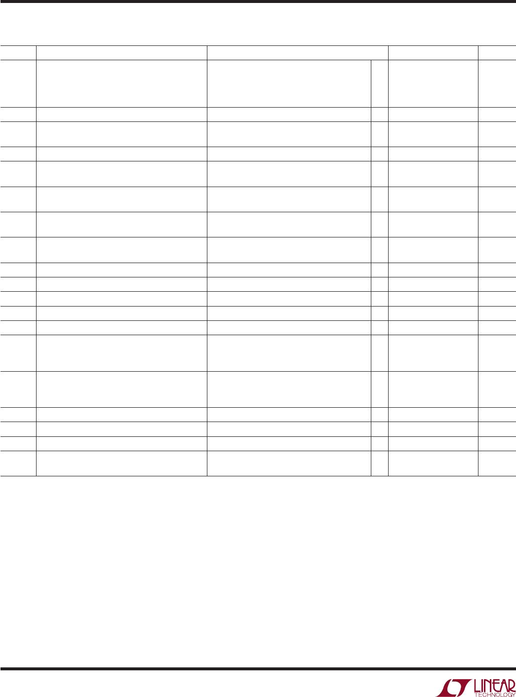
SYMBOL PARAMETER CONDITIONS MIN TYP MAX UNITS
V
OS
Input Offset Voltage V
CM
= –5V 0.5 3.5 mV
V
CM
= –5V (DD Package) 1.5 5 mV
V
CM
= –5V (SOT-23 Package) 1.5 7 mV
V
CM
= 5V 1.4 8.5 mV
V
OS
Input Offset Shift V
CM
= –5V to 3V 0.35 1.5 mV
Input Offset Voltage Match V
CM
= –5V 0.75 5.5 mV
(Channel-to-Channel) (Note 9) V
CM
= –5V (DD Package) 1.50 7.5 mV
V
OS
TC Input Offset Voltage Drift (Note 8) 10 35 µV/°C
I
B
Input Bias Current V
CM
= –4V 175 1000 nA
V
CM
= 4.8V 2.5 6 µA
Input Bias Current Match V
CM
= –4V 175 1500 nA
(Channel-to-Channel) (Note 9) V
CM
= 4.8V 175 1800 nA
I
OS
Input Offset Current V
CM
= –4V 100 1400 nA
V
CM
= 4.8V 50 1400 nA
A
VOL
Large-Signal Voltage Gain V
O
= –4V to 4V, R
L
= 1k 15 47 V/mV
V
O
= –1.5V to 1.5V, R
L
= 100 1.5 4.5 V/mV
CMRR Common Mode Rejection Ratio V
CM
= –5V to 3V 74 95 dB
CMRR Match (Channel-to-Channel) (Note 9) V
CM
= –5V to 3V 68 95 dB
Input Common Mode Range V
S
V
S
+
V
PSRR Power Supply Rejection Ratio V
S
+
= 2.5V to 10V, V
S
= 0V, V
OUT
= V
S
+
/2 65 87 dB
PSRR Match (Channel-to-Channel) (Note 9) V
S
+
= 2.5V to 10V, V
S
= 0V, V
OUT
= V
S
+
/2 59 87 dB
V
OL
Output Voltage Swing Low (Note 7) No Load 19 80 mV
I
SINK
= 5mA 100 225 mV
I
SINK
= 15mA 220 475 mV
V
OH
Output Voltage Swing High (Note 7) No Load 19 80 mV
I
SOURCE
= 5mA 150 350 mV
I
SOURCE
= 15mA 460 900 mV
I
SC
Short-Circuit Current (Note 3) 20 46 mA
I
S
Supply Current per Amplifier 2.8 3.75 mA
GBW Gain Bandwidth Product Frequency = 2MHz, R
L
= 1k 80 MHz
SR Slew Rate A
V
= –1, R
L
= 1k, V
O
= ±4V, 84 V/µs
Measured at V
O
= ±2V
8
LT1803/LT1804/LT1805
180345f
The denotes specifications which apply over the –40°C T
A
85°C
temperature range. V
S
= ±5V, V
CM
= 0V, V
OUT
= 0V unless otherwise noted. (Note 5)
ELECTRICAL CHARACTERISTICS
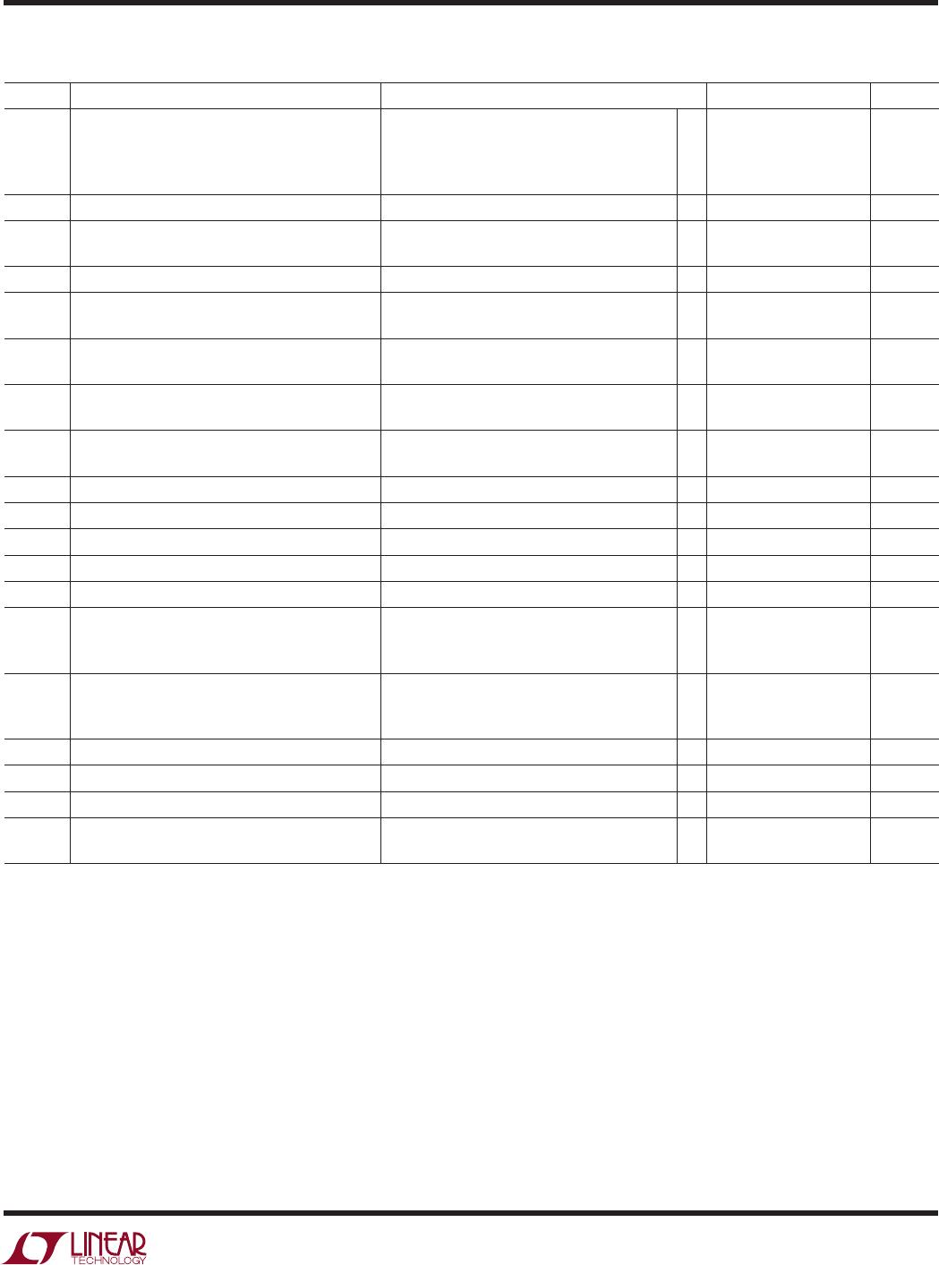
SYMBOL PARAMETER CONDITIONS MIN TYP MAX UNITS
V
OS
Input Offset Voltage V
CM
= –5V 1 4.0 mV
V
CM
= –5V (DD Package) 2 6.5 mV
V
CM
= –5V (SOT-23 Package) 28 mV
V
CM
= 5V 29 mV
V
OS
Input Offset Shift V
CM
= –5V to 3V 0.4 1.7 mV
Input Offset Voltage Match V
CM
= –5V 1 6.5 mV
(Channel-to-Channel) (Note 9) V
CM
= –5V (DD Package) 2 9.0 mV
V
OS
TC Input Offset Voltage Drift (Note 8) 10 35 µV/°C
I
B
Input Bias Current V
CM
= –4V 250 1200 nA
V
CM
= 4.8V 2.5 6.5 µA
Input Bias Current Match V
CM
= –4V 200 2000 nA
(Channel-to-Channel) (Note 9) V
CM
= 4.8V 250 2200 nA
I
OS
Input Offset Current V
CM
= –4V 100 1600 nA
V
CM
= 4.8V 50 1600 nA
A
VOL
Large-Signal Voltage Gain V
O
= –4V to 4V, R
L
= 1k 12 45 V/mV
V
O
= –1V to 1V, R
L
= 100 1.4 5.3 V/mV
CMRR Common Mode Rejection Ratio V
CM
= –5V to 3V 73 95 dB
CMRR Match (Channel-to-Channel) (Note 9) V
CM
= –5V to 3V 67 95 dB
Input Common Mode Range V
S
V
S
+
V
PSRR Power Supply Rejection Ratio V
S
+
= 2.5V to 10V, V
S
= 0V, V
OUT
= V
S
+
/2 64 86 dB
PSRR Match (Channel-to-Channel) (Note 9) V
S
+
= 2.5V to 10V, V
S
= 0V, V
OUT
= V
S
+
/2 58 86 dB
V
OL
Output Voltage Swing Low (Note 7) No Load 20 90 mV
I
SINK
= 5mA 110 250 mV
I
SINK
= 10mA 170 350 mV
V
OH
Output Voltage Swing High (Note 7) No Load 20 90 mV
I
SOURCE
= 5mA 170 400 mV
I
SOURCE
= 10mA 300 600 mV
I
SC
Short-Circuit Current (Note 3) 12.5 34 mA
I
S
Supply Current per Amplifier 2.9 4.25 mA
GBW Gain Bandwidth Product Frequency = 2MHz, R
L
= 1k 75 MHz
SR Slew Rate A
V
= –1, R
L
= 1k, V
O
= ±4V, 65 V/µs
Measured at V
O
= ±2V
Note 1: Absolute Maximium Ratings are those values beyond which the
life of the device may be impaired.
Note 2: The inputs are protected by back-to-back diodes and by ESD
diodes to supply rails. If the differential input voltage exceeds 1.4V, or if an
input is driven beyond the supply rails, the input current should be limited
to less than 10mA. This parameter is not tested; however it is guaranteed
by characterization.
Note 3: A heat sink may be required to keep the junction temperature
below the absolute maximum rating when the output is shorted
indefinitely
.
Note 4: The LT1803C/LT1803I, LT1804C/LT1804I and LT1805C/LT1805I
are guaranteed functional over the temperature range of –40°C and 85°C.
Note 5: The LT1803C/LT1804C/LT1805C are guaranteed to meet specified
performance from 0°C to 70°C. The LT1803C/LT1804C/LT1805C are
designed, characterized and expected to meet specified performance from
–40°C to 85°C but are not tested or QA sampled at these temperatures.
The LT1803I/LT1804I/LT1805I are guaranteed to meet specified perfor-
mance from –40°C to 85°C.
Note 6: Minimum supply voltage is guaranteed by power supply rejection
ratio test.
Note 7: Output voltage swings are measured between the output and
power supply rails.
Note 8: This parameter is not 100% tested.
Note 9: Matching parameters are the difference between amplifiers A and
D and between B and C on the LT1805; between the two amplifiers on the
LT1804.
Note 10: Full power bandwidth is based on slew rate:
FPBW = SR/2πV
P
9
LT1803/LT1804/LT1805
180345f
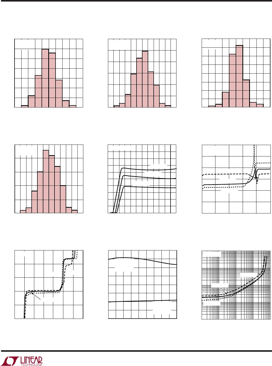
INPUT OFFSET VOLTAGE (µV)
–1250
PERCENT OF UNITS (%)
35
30
25
20
15
10
5
0
180345 G01
–750
1250750250
–250
V
S
= 5V, 0V
V
CM
= 0V
INPUT OFFSET VOLTAGE (mV)
–6
PERCENT OF UNITS (%)
30
25
20
15
10
5
0
–4
–2 0 2
180345 G02
46
V
S
= 5V, 0V
V
CM
= 5V
TOTAL SUPPLY VOLTAGE (V)
0
SUPPLY CURRENT (mA)
5.0
4.5
4.0
3.5
3.0
2.5
2.0
1.5
1.0
0.5
0
2468
180345 G05
10 12135 7911
PER AMPLIFIER
T
A
= 125°C
T
A
= 25°C
T
A
= –55°C
INPUT COMMON MODE VOLTAGE (V)
0
OFFSET VOLTAGE (µV)
2000
1500
1000
500
0
–500
–1000
1234
180345 G06
5
COMMON MODE VOLTAGE (V)
–1
INPUT BIAS CURRENT (µA)
3
2
1
0
–1
–2
1
3
4
180345 G07
0
2
5
6
V
S
= 5V, 0V
TYPICAL PART
T
A
= 125°C
T
A
= 125°C
T
A
= –55°C
T
A
= –55°C
V
S
= 5V, 0V
T
A
= 25°C
T
A
= 25°C
TEMPERATURE (°C)
–50
INPUT BIAS CURRENT (µA)
40
180345 G08
–20 10–35 –5 25 8555 70
3.0
2.5
2.0
1.5
1.0
0.5
0
–0.5
–1.0
NPN ACTIVE
V
S
= 5V, 0V
V
CM
= 5V
PNP ACTIVE
V
S
= 5V, 0V
V
CM
= 1V
LOAD CURRENT (mA)
0.01
OUTPUT SATURATION VOLTAGE (V)
0.1
1
10
0.01 1 10
180345 G09
0.001
0.1
100
V
S
= 5V, 0V
T
A
= 125°C
T
A
= –55°C
T
A
= 25°C
0
INPUT OFFSET VOLTAGE (mV)
–5
PERCENT OF UNITS (%)
40
35
30
25
20
15
10
5
0
180345 G03
–3 –2–4
54321
–1
V
S
= 5V, 0V
V
CM
= 0V
0
INPUT OFFSET VOLTAGE (mV)
–6
PERCENT OF UNITS (%)
25
20
15
10
5
0
–4
–2 0 2
180345 G04
46
V
S
= 5V, 0V
V
CM
= 5V
TYPICAL PERFOR A CE CHARACTERISTICS
UW
V
OS
Distribution, V
CM
= 0V
(SO-8, PNP Stage)
V
OS
Distribution, V
CM
= 5V
(SO-8, NPN Stage)
Supply Current vs Supply Voltage
Offset Voltage vs Input Common
Mode Voltage
Input Bias Current vs Common
Mode Voltage
Input Bias Current vs
Temperature
Output Saturation Voltage vs
Load Current (Output Low)
V
OS
Distribution, V
CM
= 0V
(SOT-23, PNP Stage)
V
OS
Distribution, V
CM
= 5V
(SOT-23, NPN Stage)

LT1803CS5#TRMPBF

Mfr. #:
Manufacturer:
Analog Devices Inc.
Description:
High Speed Operational Amplifiers 85MHz, 100V/us R-to-R In/Out OA
Lifecycle:
New from this manufacturer.
Delivery:
DHL FedEx Ups TNT EMS
Payment:
T/T Paypal Visa MoneyGram Western Union