LTC2911
10
2911f
APPLICATIONS INFORMATION
example, the PFO pin may connect to a processor non-
maskable interrupt. When the battery pack voltage drops
below the shutdown threshold, as sensed at PFI, the PFO
pin pulls low to issue an interrupt. Next, the processor
begins shutdown procedures which may include supply
sequencing and/or storage/erasure of system state in
nonvolatile memory.
Threshold Accuracy
Specifying the minimum supply voltage for a system
requires the designer to consider three factors: minimum
supply voltage for proper operation, power supply toler-
ance, and supervisor reset threshold accuracy. Highly
accurate supervisors ease the design challenge by de-
creasing the overall voltage margin required for reliable
system operation.
The reset threshold band and the power supply tolerance
bands should not overlap. This prevents false or nuisance
resets when the power supply is actually within its specified
tolerance band. The actual reset threshold of supervisors
varies over a specified band. The LTC2911 supervisor
varies ±1.5% around its nominal threshold voltage over
temperature.
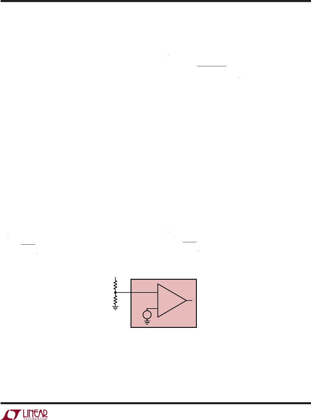
Figure 1 illustrates a typical 3.3V monitor. The LTC2911
has ±1.5% reset threshold accuracy. The nearest practical
supervisor trip point is the sum of power supply toler-
ance and the LTC2911 tolerance. So a “5%” threshold
is typically set to –6.5%, excluding resistor errors. Thus
for a 3.3V “5%” threshold, the practical supervisor trip
point is at 3.086V. The threshold is guaranteed to lie in
the band between 3.036V and 3.135V over the operating
temperature range. This 3.135V maximum threshold is at
the lower limit of supply tolerance (3.3V – 5%) to prevent
false tripping.
The system must operate reliably a little below 3.036V
(or 3.3V, –8%), or risk malfunction before a reset signal
is properly issued. A less accurate supervisor increases
the supply voltage tolerance requirements and the risk
of system malfunction. The LTC2911’s ±1.5% threshold
voltage specification minimizes these requirements.
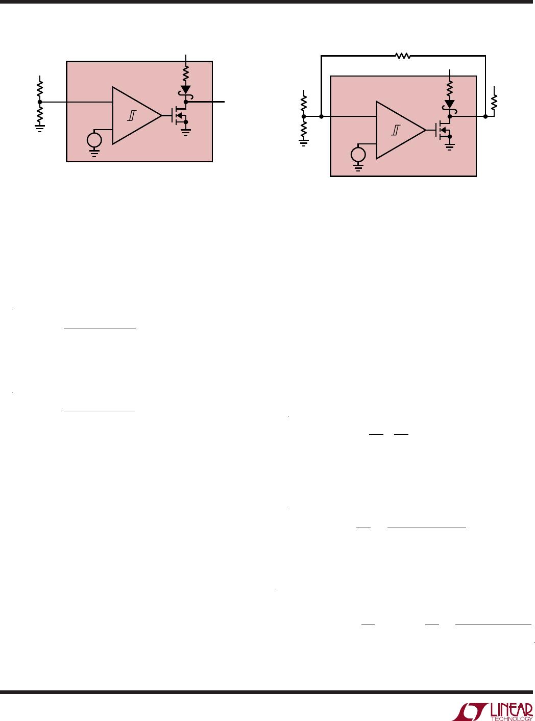
V1 and V2 Supply Monitors
All the LTC2911 options have a V1 threshold equal to
3.086V (3.3V – 6.5%). The V2 thresholds are 4.675V
(5V – 6.5%), 2.338V (2.5V – 6.5%), 1.683V (1.8V – 6.5%)
and 1.122V (1.2V – 6.5%) for options LTC2911-1,
3.3V
3.135V
±1.5%
THRESHOLD
BAND
3.086V
3.036V
REGION OF POTENTIAL MALFUNCTION
–5%
SUPPLY TOLERANCE
IDEAL
SUPERVISOR
THRESHOLD
MINIMUM
RELIABLE
SYSTEM
VOLTAGE
NOMINAL
SUPPLY
VOLTAGE
–6.5%
–8%
2911 F01
Figure 1. 1.5% Threshold Accuracy Improves System Reliability
LTC2911
11
2911f
LTC2911-2, LTC2911-3 and LTC2911-4 respectively. V2
of the LTC2911-5 option is a high impedance input with
a nominal 0.5V threshold.
Input Noise Filtering for RST
The V1, V2 and ADJ comparators have a response time that
is inversely proportional to overdrive. This characteristic
is illustrated in the Typical Performance Characteristics
as the graph Allowable Glitch Duration versus Overdrive.
The ADJ and the LTC2911-5’s V2 pin may be bypassed
with a capacitor to increase the filtering in applications that
demand it. The resultant RC lowpass filter at the inputs will
further reject high frequency components, at the cost of
slowing the monitors response to fault conditions.
Resistor Selection for ADJ
The threshold of the supply monitored by the ADJ pin is
configured with an external resistive divider (R2 and R1)
connected between the supply and ground. The tap point
for the divider is connected to the adjustable input (ADJ)
which has a 0.5V threshold. (See Figure 2)
Normally, the user selects a trip voltage based on the sup-
ply and acceptable tolerances, and a value of R1 based on
current drawn. For a given current, I, R1 is given by:
R1=
0.5V
I
To minimize errors arising from the ADJ input bias current,
a value of less than 100k is recommended for R1.
R2 is then chosen by:
R2 = R1
V
TRIP_ ADJ
0.5V
1
where, V
TRIP_ADJ
is the supply threshold when the ADJ
pin falls below its 0.5V threshold.
For accurate monitoring, the resistor tolerance should be
as small as possible. Resistor tolerance of 0.1% or some
trimming of components should be considered for R2/R1
in applications that require an accurate trip point.
Resistor Selection for PFI
An external resistive divider (R3 and R4) connected between
the supply and ground configures the threshold of the
supply monitored by the power-fail comparator. The tap
point for the divider is connected to the PFI input which
has a 0.5V threshold. (See Figure 3a)
Resistor selection follows a process similar to that for
the ADJ pin.
R3 is given by:
R3 =
0.5V
I
APPLICATIONS INFORMATION
+
+
0.5V
2911 F02
ADJ
LTC2911
R2
R1
V
TRIP
Figure 2. Setting the Adjustable (ADJ) Trip Point
LTC2911
12
2911f
Again, to minimize errors arising from the PFI input bias
current, a value of less than 100k is recommended for
R3.
R4 can be chosen either using the PFI falling threshold or
the PFI rising threshold.
For the falling edge threshold, use the equation:
R4 = R3
V
TRIP_ PFI_FALL
0.5V
1
Alternatively, for the rising edge threshold, use the
equation:
R4 = R3
V
TRIP_ PFI_RISE
0.515V
1
where V
TRIP_PFI_FALL
is the supply threshold when the PFI
pin falls below the 0.5V falling threshold, and V
TRIP_PFI_RISE
is the supply threshold when the PFI pin rises above the
0.515V rising threshold.
Note that V
TRIP_PFI_RISE
is typically 3% above the
V
TRIP_PFI_FALL
due to the fact that the PFI 515mV rising
threshold is 3% above its 500mV falling threshold.
In applications that require an accurate trip point, the R4
and R3 resistors should have small tolerances.
Hysteresis for Power-Fail Comparator
The power-fail comparator uses a positive 3% accurate
hysteresis to combat spurious triggering while maintain-
ing accurate thresholds for both the rising and falling
edges. The nominal threshold is 500mV at the falling edge
and 515mV at the rising edge. The hysteresis prevents
oscillation when the monitored voltage passes through
the thresholds. If the PFI pin is connected to an external
resistive divider, it may be bypassed with a capacitor for
additional noise filtering.
Increasing the Power-Fail Hysteresis
The power-fail comparator hysteresis can be increased by
adding two resistors, R5 and R6, as shown in Figure 3b.
When PFO is low, R5 sinks current from the center tap
of the R3 and R4 resistive divider. The upper threshold is
therefore given by:
V
H
= 0.515V 1+
R4
R3
+
R4
R5
When PFO is high, the series combination of R5 and R6
sources current into the center tap of the R3 and R4 resis-
tive divider. This leads to a lower threshold of:
V
L
= 0.5V 1+
R4
R3
3.3V 0.5V
( )
R4
R5+ R6
The addition of R5 and R6 increases the hysteresis to:
V
HYST
= V
H
V
L
= 0.015 1+
R4
R3
+ 0.515
R4
R5
+
3.3V 0.5V
( )
R4
R5+ R6
APPLICATIONS INFORMATION
Figure 3a. Setting the Power-Fail (PFI) Trip Point
+
+
0.5V
2911 F03a
PFI
V1
114k
PFO
LTC2911
R4
R3
V
TRIP
Figure 3b. Increasing Power-Fail Hysteresis
+
+
0.5V
2911 F03b
PFI
V1
V1
PFO
LTC2911
R4
R6
R5
R3
V
TRIP
114k

LTC2911CTS8-1#TRPBF

Mfr. #:
Manufacturer:
Analog Devices Inc.
Description:
Supervisory Circuits Precision Tripply Supply Supervisor with Power-Fail Comparator (3.3V, 5V, ADJ)
Lifecycle:
New from this manufacturer.
Delivery:
DHL FedEx Ups TNT EMS
Payment:
T/T Paypal Visa MoneyGram Western Union