LTC2911
4
2911f
ELECTRICAL CHARACTERISTICS
The l denotes the specifications which apply over the full operating
temperature range, otherwise specifications are at T
A
= 25°C. V
ADJ
= 0.55V, V
PFI
= 0.55V, V1 = 3.3V unless otherwise noted. (Notes 2, 3)
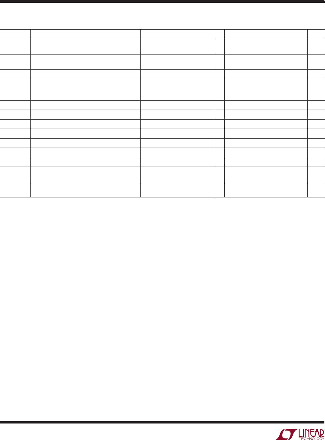
SYMBOL PARAMETER CONDITIONS MIN TYP MAX UNITS
t
P,PF
PFI Comparator Propagation Delay to PFO V
PFI
Driven Beyond Threshold
V
PFT
by More Than 10%
l
8 30 80 µs
t
UV
V1, V2, ADJ Undervoltage Detect to RST Low V
X
Less Than Threshold V
RTX
by
More Than 10%
l
8 30 80 µs
V
OH
RST, PFO Output Voltage High (Note 5) I
RST
= –1µA
l
V1 – 1 V1 V
V
OL
RST, PFO Output Voltage Low (Note 6) V
CC
= 0.5V, I = 5µA
V
CC
= 1V, I = 100µA
V
CC
= 3V, I = 2.5mA
l
l
l
0.01
0.01
0.10
0.15
0.15
0.30
V
V
V
t
RST(EXT)
Reset Timeout Period, External C
TMR
= 2.2nF
l
15 20 27 ms
t
RST(INT)
Reset Timeout Period, Internal V
TMR
= V1
l
140 200 280 ms
V
TMR(INT)
Timer Internal Mode Threshold V
TMR
Rising
l
V1 – 0.40 V1 – 0.020 V1 – 0.10 V
V
TMR(INT)
Timer Internal Mode Hysteresis V
TMR
Falling
l
40 100 160 mV
V
TMR(LATCH)
Timer Latch Mode Threshold V
TMR
Falling
l
0.10 0.20 0.40 V
V
TMR(LATCH)
Timer Latch Mode Hysteresis V
TMR
Rising
l
40 75 160 mV
t
P, LR
Latch Release Propagation Delay to RST Low V
TMR
Rising, Step 0V to 0.6V
l
0.5 3 µs
t
SU,MON
Monitor Input Setup Time to Latch Enable (Note 7)
Monitor Input Setup Time to Latch Release
V
TMR
Falling, Step 0.6V to 0V
V
TMR
Rising, Step 0V to 0.6V
l
2 ms
t
HD, MON
Monitor Input Hold Time to Latch Enable
Monitor Input Hold Time to Latch Release
V
TMR
Falling, Step 0.6V to 0V
V
TMR
Rising, Step 0V to 0.6V
l
0 µs
Note 1: Stresses beyond those listed under Absolute Maximum Ratings
may cause permanent damage to the device. Exposure to any Absolute
Maximum Rating condition for extended periods may affect device
reliability and lifetime.
Note 2: All currents into pins are positive; all voltages are referenced to
GND unless otherwise noted.
Note 3: The internal supply voltage (V
CC
) is generated from the greater of
the voltages on the V1 and V2 inputs. V
CC
= V1 for the LTC2911-5.
Note 4: Under typical operating conditions, quiescent current is drawn
from the greater of the voltages on the V1 and V2 inputs. For the
LTC2911-5 only V1 supplies the quiescent current.
Note 5: The RST and PFO output pins on the LTC2911 have internal pull-
ups to V1. However, for faster rise times or for V
OH
voltages greater than
V1, use an external pull-up resistor.
Note 6: The RST and PFO pull-down currents are derived from V1 and V2
except for the LTC2911-5 where the pull-down strength is derived only
from V1.
Note 7: t
SU,MON
is required to latch a low RST state and t
SU,MON
+ t
RST
is
required to latch a high RST state.
LTC2911
5
2911f
TYPICAL PERFORMANCE CHARACTERISTICS
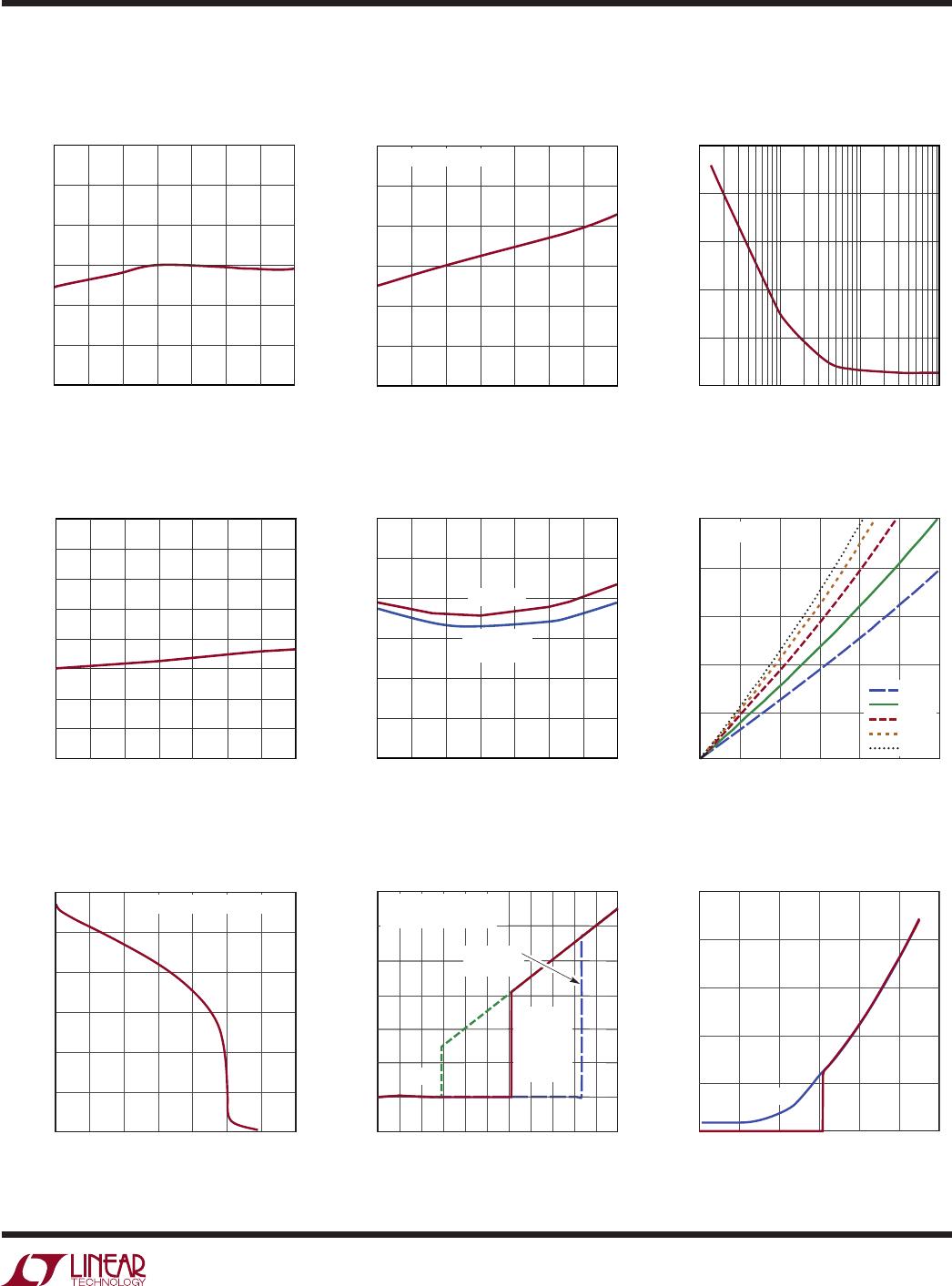
PFI Hysteresis vs Temperature
Reset Timeout Period vs
Temperature
RST, PFO Voltage Output Low
vs Sink Current
RST, PFO Voltage Output High
vs Source Current
RST, PFO Voltage Output High
vs V
CC
RST, PFO Pin Source Current
vs V1
Normalized Reset and Power-Fail
Threshold Voltages vs Temperature
Quiescent Supply Current
vs Temperature
Allowable Glitch Duration
vs Overdrive
TEMPERATURE (°C)
–50
0.985
NORMALIZED THRESHOLD VOLTAGE (V/V)
0.990
0.995
1.000
1.005
0 50
100
125
2911 G01
1.010
1.015
–25 25
75
TEMPERATURE (°C)
–50
0
QUIESCENT SUPPLY CURRENT (µA)
10
20
30
40
0 50
100
125
2911 G02
50
60
–25 25
75
I
V2
FOR LTC2911-1
OVERDRIVE (%)
0.1
0
GLITCH DURATION (µs)
300
400
500
1 10 100
2911 G03
200
100
T
AMB
(°C)
–50
HYSTERESIS (mV)
16.0
17.0
125
2911 G04
15.0
14.0
0
50
100
–25
25
75
18.0
15.5
16.5
14.5
17.5
TEMPERATURE (°C)
–50
140
TIMEOUT PERIOD (ms)
160
180
200
220
0 50
100
125
2911 G05
240
260
–25 25
75
INTERNAL
EXTERNAL
C
TMR
= 22nF
SINK CURRENT (mA)
0
0
VOLTAGE OUTPUT LOW (V)
0.2
0.4
0.6
0.8
1.0
5
10 15 20
2911 G06
25 30
–40°C
25°C
85°C
125°C
150°C
V
CC
= 3V
SOURCE CURRENT (µA)
0
2.0
2.5
15 25
2911 G07
1.5
1.0
5 10
20 30
35
0.5
0
V1 = 3.135V, V2 = 5V FOR RST
V
CC
(V)
0
–1
VOLTAGE OUTPUT HIGH (V)
0
2
3
4
6
0.5
2.5
3.5
2911 G08
1
5
2
4.5
5.55
1
1.5
3 4
V1 = V2 = ADJ = PFI
10k PULL-UP TO V
CC
RST FOR
LTC2911-1
RST FOR
LTC2911-2
LTC2911-3
LTC2911-4
LTC2911-5
PFO
V1 (V)
OUTPUT SOURCE CURRENT (µA)
60
80
100
2911 G09
40
20
0
10 5 6
2
3
4
RST
PFO
LTC2911
6
2911f
PIN FUNCTIONS
ADJ: Adjustable Voltage Monitor Input. Input to a voltage
monitor comparator with a 0.5V nominal threshold. Tie
to V1 if unused.
Exposed Pad (DFN Only): Exposed pad may be left open
or connected to device ground.
GND: Device Ground.
PFI: Power-Fail Voltage Monitor Input. Input to the power-
fail comparator with a 500mV threshold at the falling
edge and a 515mV threshold at the rising edge, giving
a 3% hysteresis for noise rejection. Tie to V1 or GND if
unused.
PFO: Power-Fail Logic Output. This pin asserts low when
the PFI input voltage is below its threshold and goes high
when the PFI input voltage is above its threshold. This pin
provides a weak pull-up current to V1. This current is typi-
cally 29µA at V1 = 3.3V. The pin can be pulled to voltages
higher than V1 by external pull-up resistors. PFO provides
an early warning signal of a system power failure.
RST: Reset Logic Output. This pin asserts low when any
of the V1, V2, or ADJ inputs are below their reset thresh-
olds. Pulls high when all the monitored inputs are above
their thresholds for longer than a timeout period. This pin
provides a weak pull-up current to V1. This current is typi-
cally 29µA at V1 = 3.3V. The pin can be pulled to voltages
higher than V1 by external pull-up resistors. The status of
RST can be latched by holding the TMR pin at GND.
TMR: Reset Timeout Control. Attach an external capacitor,
C
TMR
, to GND to set a reset timeout period of 9.4ms/nF. A
low leakage ceramic capacitor is recommended for timer
accuracy. A 2.2nF capacitor generates a 20ms timeout.
Leaving the TMR pin open without a capacitor generates
a minimum timeout of approximately 400µs which will
vary depending on the parasitic capacitance on the pin.
Tying this pin to V1 enables the internal 200ms timeout.
Pulling this pin to GND latches the reset state.
V1: 3.3V Monitor and Power Supply Input. V1 is an accu-
rate 3.3V, –5% undervoltage supply monitor. The internal
V
CC
is generated from the greater of the voltages at the
V1 and V2 inputs for the LTC2911-1/LTC2911-2/LTC2911-
3/LTC2911-4 options. The LTC2911-5 option always derives
its power supply from the V1 pin. Bypass this pin to GND
with a 0.1µF (or greater) capacitor for the LTC2911-2
through LTC2911-5.
V2: Voltage Monitor and Power Supply Input. V2 is a
–5% undervoltage supply monitor for a 5V, 2.5V, 1.8V
or 1.2V supply for the LTC2911-1/LTC2911-2/LTC2911-
3/LTC2911-4 options, respectively. Because the internal
V
CC
is generated from the greater of the V1 and V2 inputs
for these options, the V2 pin should be bypassed to GND
with a 0.1µF (or greater) capacitor for the LTC2911-1. The
V2 pin of the LTC2911-5 is a high impedance input with a
0.5V threshold, allowing the trip threshold of the monitored
supply to be configured with a resistive divider.
LTC2911CTS8-1#TRPBF

Mfr. #:
Manufacturer:
Analog Devices Inc.
Description:
Supervisory Circuits Precision Tripply Supply Supervisor with Power-Fail Comparator (3.3V, 5V, ADJ)
Lifecycle:
New from this manufacturer.
Delivery:
DHL FedEx Ups TNT EMS
Payment:
T/T Paypal Visa MoneyGram Western Union