LTC2911
15
2911f
Output Pin Characteristics
The DC characteristics of the RST and PFO pull-down
strength are shown in the Typical Performance Character-
istics. The circuits that drive the pull-down of the output
pins are powered by the internal V
CC
(the greater voltage
of V1 or V2). During power-up, a V
CC
of at least 0.5V en-
sures a low output state. The V
OL
voltage depends on the
current sunk by RST and PFO as shown in the Figure 8.
The open-drain nature of the RST and PFO pins allows for
wire-ORed connections. For example, multiple LTC2911s
may be wire-ORed to monitor additional supplies, or open-
drain logic can be connected to allow other conditions to
issue the reset and/or power-fail signals.
Output Pin Rise and Fall Time
The open-drain output pins (RST and PFO) contain weak
pull-up circuitry to V1. Use an external pull-up resistor
when the outputs need to pull beyond V1 and/or require
a faster rise time. Use external pull-up resistor values of
100k or less.
When output pins are externally pulled up to voltages higher
than V1, an internal network automatically protects the
weak pull-up circuitry from reverse currents. For a given
external load capacitance or C
LOAD
, the rise and fall times
can be estimated using Figure 9. The output pins have very
strong pull-down capability. With a 150pF load capacitance
the reset line can pull down in about 30ns.
During power-up, with a capacitor connected to the TMR
pin, the part remains in the reset latch mode described
above until the 2.2µA flowing out of the TMR pin charges
the capacitor beyond the V
TMR(LATCH)
threshold. For this
reason, large capacitors will extend the RST timeout during
power-up. For example, if C
TMR
= 1µF, the LTC2911 leaves
the reset latch mode 90ms after power-up and the RST
pin goes high after a 9 second timeout.
Figures 7a and 7b show how the TMR pin can be driven
low to latch the state of the RST pin or floated or driven
high for external and internal reset timing, respectively.
TMR
2911 F07a
SYSTEM
LOGIC
TMR
V1
2911 F07b
SYSTEM
LOGIC
Figure 7a. Open-Drain (or Three-State Buffer) Output.
Grounds TMR to Latch the State of RST. Floats TMR for
External Reset Timing
Figure 7b. V1 Powered Inverter. Grounds TMR
to Latch the State of RST. Drives TMR High for
Internal Reset Timing
APPLICATIONS INFORMATION
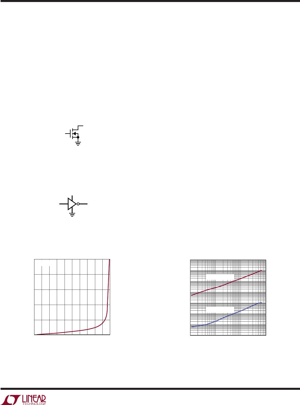
I
SINK
(µA)
0
VOLTAGE OUTPUT LOW (mV)
1200
1600
2000
80
2911 F08
800
400
0
2010
4030
60 70 90
50
100
V
CC
= 0.5V
Figure 8. Voltage Output Low vs I
SINK
at V
CC
= 0.5V
C
LOAD
(F)
10n
t
FALL
OR t
RISE
(s)
1µ
100µ
100n
10µ
1m
10m
100p 1n 10n
2911 F09
1n
10p
t
RISE
LTC2911-1
t
FALL
LTC2911-1
Figure 9. t
RISE
and t
FALL
vs C
LOAD

