AMIS−49587
www.onsemi.com
10
CRC
CRC is a 5V compliant open drain output. An external pull−up resistor defines the logic high level as illustrated in Figure 5.
A typical value for this pull−up resistance “R” is 10 kW. The signal on this output depends on the cyclic redundancy code result
of the received frame. If the cyclic redundancy code is correct CRC = 1 during the pause between 2 time slots.
RESB
RESB is a digital input pin. It is used to perform a hardware reset of the AMIS−49587. This pin supports a 5 V voltage level.
The reset is active when the signal is low (0 V).
TEST
TEST is a digital input pin. It is used to enable the test mode of the chip. Normal mode is activated when TEST signal is low
(0 V). For normal operation, the TEST pin may be left unconnected. Due to the internal pulldown, the signal is maintained to
low (0 V). TEST pin is not 5 V safe.
TX_ENB
TX_ENB is a digital output pin. It is low when the transmitter is activated. The signal is available to turn on the line driver.
TX_ENB is a 5 V safe with open drain output, hence a pull−up resistance is necessary achieve the requested voltage level
associated with a logical one. See also Figure 5 for reference.
TX_OUT
TX_OUT is the analog output pin of the transmitter. The provided signal is the S−FSK modulated frames. A filtering operation
must be performed to reduce the second order harmonic distortion. For this purpose an active filter is realized. Figure 7 gives
the representation of this filter.
Figure 7. TX_OUT Filter
ALC
control
ALC_IN
Transmitter (S−FSK Modulator)
ARM
Interface
&
Control
TX_OUT
LP
Filter
TX_EN
TO TX POWER
OUTPUT STAGE
FROM LINE
DRIVER
C
1
R
1
V
SSA
C
2
R
2
R
3
C
3
C
4
ALC_IN
ALC_IN is the automatic level control analog input pin. The signal is used to adjust the level of the transmitted signal. The
signal level adaptation is based on the AC component. The DC level on the ALC_IN pin is fixed internally to 1.65 V. Comparing
the peak voltage of the AC signal with two internal thresholds does the adaptation of the gain. Low threshold is fixed to 0.4 V.
A value under this threshold will result in an increase of the gain. The high threshold is fixed to 0.6 V. A value over this threshold
will result in a decrease of the gain. A serial capacitance is used to block the DC components. The level adaptation is performed
during the transmission of the first two bits of a new frame. Eight successive adaptations are performed.
AMIS−49587
www.onsemi.com
11
4 ELECTRICAL CHARACTERISTICS
4.1 DC AND AC CHARACTERISTICS
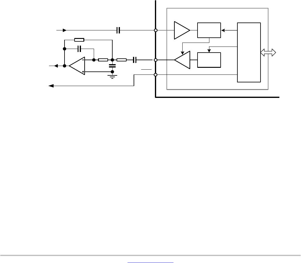
4.1.1 Oscillator: Pin XIN, XOUT
In production the actual oscillation of the oscillator and duty cycle will not be tested. The production test will be based on the
static parameters and the inversion from XIN to XOUT in order to guarantee the functionality of the oscillator.
Table 8. OSCILLATOR
Parameter Test Conditions Symbol Min Typ Max Unit
Crystal frequency (Note 1) f
CLK
−100 ppm 24 +100 ppm MHz
Duty cycle with quartz connected (Note 1) 40 61 %
Start−up time (Note 1) T
startup
50 ms
Maximum Capacitive load on XOUT XIN used as clock input CL
XOUT
50 pF
Low input threshold voltage XIN used as clock input VIL
XOUT
0.3 V
DD
V
High input threshold voltage XIN used as clock input VIH
XOUT
0.7 V
DD
V
Low output voltage XIN used as clock input,
XOUT = 2 mA
VOL
XOUT
0.3 V
High input voltage XIN used as clock input VOH
XOUT
V
DD
−0.3 V
1. Guaranteed by design. Maximum allowed series loss resistance up to 80 W.
4.1.2 Zero Crossing Detector and 50/60 Hz PLL: Pin M50HZ_IN
Table 9. ZERO CROSSING DETECTOR AND 50/60 Hz PLL
Parameter Test Conditions Symbol Min Typ Max Unit
Maximum peak input current Imp
M50HZIN
−20 20 mA
Maximum average input current During 1 ms Imavg
M50HZIN
−2 2 mA
Mains voltage (ms) range With protection resistor at
M50HZIN
V
MAINS
90 550 V
Rising threshold level (Note 2) VIRM
50HZIN
1.9 V
Falling threshold level (Note 2) VIFM
50HZIN
0.82 V
Hysteresis (Note 2) VHY
50HZIN
0.4 V
Lock range for 50 Hz (Note 3) MAINS_FREQ = 0 (50 Hz) Flock
50Hz
45 55 Hz
Lock range for 60 Hz (Note 3) MAINS_FREQ = 0 (60 Hz) Flock
60Hz
54 66 Hz
Lock time (Note 3) MAINS_FREQ = 0 (50 Hz) Tlock
50Hz
15 s
Lock time (Note 3) MAINS_FREQ = 0 (60 Hz) Tlock
60Hz
20 s
Frequency variation without going out of
lock (Note 3)
MAINS_FREQ = 0 (50 Hz) DF
60Hz
0.1 Hz/s
Frequency variation without going out of
lock (Note 3)
MAINS_FREQ = 0 (60 Hz) DF
50Hz
0.1 Hz/s
Jitter of CHIP_CLK (Note 3) Jitter
CHIP_CLK
−25 25
ms
2. Measured relative to V
SS
.
3. These parameters will not be measured in production since the performance is totally dependent of a digital circuit which will be guaranteed
by the digital test patterns.
AMIS−49587
www.onsemi.com
12
4.1.3 Transmitter External Parameters: Pin TX_OUT, ALC_IN, TX_ENB
To guarantee the transmitter external specifications the TX_CLK frequency must be 12 MHz $ 100 ppm.
Table 10. TRANSMITTER EXTERNAL PARAMETERS
Parameter Test Conditions Symbol Min Typ Max Unit
Maximum peak output level fTX_OUT = 23.75 kHz
fTX_OUT = 95 kHz
Level control at max. output
V
TX_OUT
0.85
0.76
1.15
1.22
Vp
Second order harmonic distortion fTX_OUT = 95 kHz
Level control at max. output
HD2 −54 dB
Third order harmonic distortion fTX_OUT = 95 kHz
Level control at max. output
HD3 −56 dB
Frequency accuracy of the
generated sine wave
(Notes 4 and 6) Df
TX_OUT
30 Hz
Capacitive output load at pin
TX_OUT
(Note 4) CL
TX_OUT
20 pF
Resistive output load at pin
TX_OUT
RL
TX_OUT
5
kW
Turn off delay of TX_ENB output (Note 5) Td
TX_ENB
0.25 0.5 ms
Automatic level control attenuation
step
ALC
step
2.9 3.1 dB
Maximum attenuation ALC
range
20.3 21.7 dB
Low threshold level on ALC_IN VTL
ALC_IN
−0.49 −0.36 V
High threshold level on ALC_IN VTH
ALC_IN
−0.71 −0.54 V
Input impedance of ALC_IN pin R
ALC_IN
111 189
kW
Power supply rejection ration of the
transmitter section
PSRR
TX_OUT
10 (Note 7) 35 (Note 8) dB
4. This parameter will not be tested in production.
5. This delay corresponds to the internal transmit path delay and will be defined during design.
6. Taking into account the resolution of the DDS and an accuracy of 100 ppm of the crystal.
7. A sinusoidal signal of 10 kHz and 100 mVpp is injected between VDDA and VSSA. The digital AD converter generates an idle pattern. The
signal level at TX_OUT is measured to determine the parameter.
8. A sinusoidal signal of 50 Hz and 100 mVpp is injected between VDDA and VSSA. The digital AD converter generates an idle pattern. The
signal level at TX_OUT is measured to determine the parameter.
The LPF filter + amplifier must have a frequency characteristic between the limits listed below. The absolute output level
depends on the operating condition. In production the measurement will be done for relative output levels where the 0 dB
reference value is measured at 50 kHz with a signal amplitude of 100 mV.
Table 11. TRANSMITTER FREQUENCY CHARACTERISTICS
Frequency (kHz)
Attenuation
Unit
Min Max
10 −0.5 0.5 dB
95 −1.3 0.5 dB
130 −4.5 −2.0 dB
165 −3.0 dB
330 −18.0 dB
660 −36.0 dB
1000 −50 dB
2000 −50 dB

AMIS49587C5871G

Mfr. #:
Manufacturer:
ON Semiconductor
Description:
Network Controller & Processor ICs C587- NAF- AMIS49587
Lifecycle:
New from this manufacturer.
Delivery:
DHL FedEx Ups TNT EMS
Payment:
T/T Paypal Visa MoneyGram Western Union